PIC18F6525/6621/8525/8621
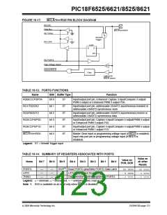
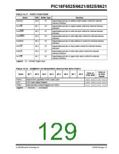
TABLE 10-15: PORTH FUNCTIONS
Name
RH0/A16
Bit#
Buffer Type
Function
bit 0
bit 1
bit 2
bit 3
bit 4
ST/TTL(1)
ST/TTL(1)
ST/TTL(1)
ST/TTL(1)
ST
Input/output port pin or address bit 16 for external memory interface.
Input/output port pin or address bit 17 for external memory interface.
Input/output port pin or address bit 18 for external memory interface.
Input/output port pin or address bit 19 for external memory interface.
RH1/A17
RH2/A18
RH3/A19
RH4/AN12/P3C(2)
Input/output port pin, analog input channel 12 or Enhanced PWM
output P3C.
RH5/AN13/P3B(2)
RH6/AN14/P1C(2)
RH7/AN15/P1B(2)
bit 5
bit 6
bit 7
ST
ST
ST
Input/output port pin, analog input channel 13 or Enhanced PWM
output P3B.
Input/output port pin, analog input channel 14 or Enhanced PWM
output P1C.
Input/output port pin, analog input channel 15 or Enhanced PWM3
output P1B.
Legend: ST = Schmitt Trigger input, TTL = TTL input
Note 1: Input buffers are Schmitt Triggers when in I/O mode and TTL buffers when in System Bus or Parallel Slave
Port mode.
2: Valid only for PIC18F8525/8621 devices when ECCPMX is not set. The alternate assignments for
P1B/P1C/P3B/P3C in all PIC18F6525/6621 devices and in PIC18F8525/8621 devices when ECCPMX is
set are RE6, RE5, RE4 and RE3, respectively.
TABLE 10-16: SUMMARY OF REGISTERS ASSOCIATED WITH PORTH
Value on
Value on:
POR, BOR
Name
Bit 7
Bit 6
Bit 5
Bit 4
Bit 3
Bit 2
Bit 1
Bit 0
all other
Resets
1111 1111
0000 xxxx
xxxx xxxx
--00 0000
0-00 --00
1111 1111
0000 uuuu
uuuu uuuu
--00 0000
0-00 --00
TRISH
PORTH Data Direction Control Register
Read PORTH pin/Write PORTH Data Latch
PORTH
LATH
Read PORTH Data Latch/Write PORTH Data Latch
ADCON1
MEMCON(1) EBDIS
—
—
—
VCFG1 VCFG0 PCFG3 PCFG2 PCFG1 PCFG0
WAIT1 WAIT0 WM1 WM0
—
—
Legend: x= unknown, u= unchanged, — = unimplemented, read as ‘0’. Shaded cells are not used by PORTH.
Note 1: This register is unused on PIC18F6525/6621 devices and reads as ‘0’.
DS39612B-page 124
2005 Microchip Technology Inc.

 MICROCHIP [ MICROCHIP ]