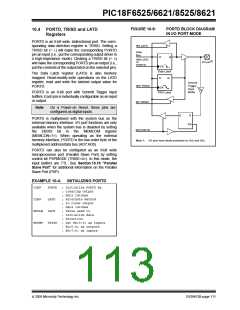
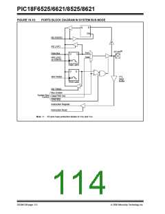
PIC18F6525/6621/8525/8621
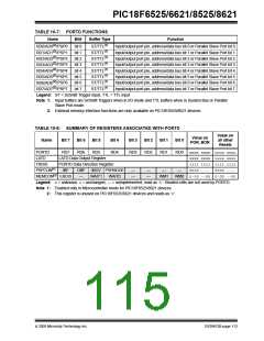
TABLE 10-5: PORTC FUNCTIONS
Name
Bit# Buffer Type
Function
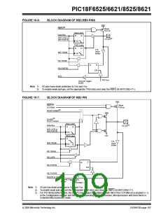
RC0/T1OSO/T13CKI bit 0
ST
Input/output port pin, Timer1 oscillator output or Timer1/Timer3 clock
input.
RC1/T1OSI/
bit 1
ST
Input/output port pin, Timer1 oscillator input, Enhanced Capture 2
input/Compare 2 output/PWM 2 output or Enhanced PWM output
P2A.
ECCP2(1)/P2A(1)
RC2/ECCP1/P1A
RC3/SCK/SCL
bit 2
bit 3
ST
ST
Input/output port pin, Enhanced Capture 1 input/Compare 1 output/
PWM 1 output or Enhanced PWM output P1A.
RC3 can also be the synchronous serial clock for both SPI™ and
I2C™ modes.
RC4/SDI/SDA
RC5/SDO
bit 4
bit 5
bit 6
ST
ST
ST
RC4 can also be the SPI data in (SPI mode) or data I/O (I2C mode).
Input/output port pin or synchronous serial port data output.
RC6/TX1/CK1
Input/output port pin, Addressable USART1 Asynchronous Transmit
or Addressable USART1 Synchronous Clock.
RC7/RX1/DT1
bit 7
ST
Input/output port pin, Addressable USART1 Asynchronous Receive or
Addressable USART1 Synchronous Data.
Legend: ST = Schmitt Trigger input
Note 1: Valid when CCP2MX is set in all devices and in all operating modes (default). RE7 is the alternate assignment
for ECCP2/P2A for all PIC18F6525/6621 devices and PIC18F8525/8621 devices in Microcontroller modes
when CCP2MX is not set; RB3 is the alternate assignment for PIC18F8525/8621 devices in all other operating
modes.
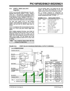
TABLE 10-6: SUMMARY OF REGISTERS ASSOCIATED WITH PORTC
Value on
Value on
POR, BOR
Name
Bit 7
Bit 6
Bit 5
Bit 4
Bit 3
Bit 2
Bit 1
Bit 0
all other
Resets
PORTC
LATC
RC7
RC6
RC5
RC4
RC3
RC2
RC1
RC0
xxxx xxxx uuuu uuuu
xxxx xxxx uuuu uuuu
1111 1111 1111 1111
LATC Data Output Register
PORTC Data Direction Register
TRISC
Legend: x= unknown, u= unchanged
DS39612B-page 110
2005 Microchip Technology Inc.

 MICROCHIP [ MICROCHIP ]