PIC18F6525/6621/8525/8621
A mismatch condition will continue to set flag bit, RBIF.
Reading PORTB will end the mismatch condition and
allow flag bit RBIF to be cleared.
10.2 PORTB, TRISB and LATB
Registers
PORTB is an 8-bit wide, bidirectional port. The corre-
sponding data direction register is TRISB. Setting a
TRISB bit (= 1) will make the corresponding PORTB
pin an input (i.e., put the corresponding output driver in
a high-impedance mode). Clearing a TRISB bit (= 0)
will make the corresponding PORTB pin an output (i.e.,
put the contents of the output latch on the selected pin).
The interrupt-on-change feature is recommended for
wake-up on key depression operation and operations
where PORTB is only used for the interrupt-on-change
feature. Polling of PORTB is not recommended while
using the interrupt-on-change feature.
For PIC18F8525/8621 devices, RB3 can be configured
by the configuration bit, CCP2MX, as the alternate
peripheral pin for the ECCP2 module. This is only
available when the device is configured in
Microprocessor, Microprocessor with Boot Block or
Extended Microcontroller operating modes.
The Data Latch register (LATB) is also memory
mapped. Read-modify-write operations on the LATB
register, read and write the latched output value for
PORTB.
The RB5 pin is used as the LVP programming pin.
When the LVP configuration bit is programmed, this pin
loses the I/O function and becomes a programming test
function.
EXAMPLE 10-2:
INITIALIZING PORTB
CLRF
PORTB
; Initialize PORTB by
; clearing output
; data latches
CLRF
LATB
; Alternate method
; to clear output
; data latches
Note:
When LVP is enabled, the weak pull-up on
RB5 is disabled.
MOVLW
MOVWF
0xCF
; Value used to
; initialize data
; direction
; Set RB<3:0> as inputs
; RB<5:4> as outputs
; RB<7:6> as inputs
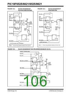
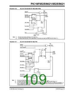
FIGURE 10-5:
BLOCK DIAGRAM OF
RB7:RB4 PINS
TRISB
VDD
RBPU(2)
Data Bus
Weak
P
Pull-up
Each of the PORTB pins has a weak internal pull-up. A
single control bit can turn on all the pull-ups. This is
performed by clearing bit RBPU (INTCON2<7>). The
weak pull-up is automatically turned off when the port
pin is configured as an output. The pull-ups are
disabled on a Power-on Reset.
Data Latch
D
Q
WR LATB
or PORTB
I/O pin(1)
CK
TRIS Latch
D
Q
Note:
On a Power-on Reset, these pins are
configured as digital inputs.
WR TRISB
TTL
Input
Buffer
CK
ST
Buffer
Four of the PORTB pins (RB3:RB0) are the external
interrupt pins, INT3 through INT0. In order to use these
pins as external interrupts, the corresponding TRISB
bit must be set to ‘1’.
RD TRISB
RD LATB
The other four PORTB pins (RB7:RB4) have an
interrupt-on-change feature. Only pins configured as
inputs can cause this interrupt to occur (i.e., any
RB7:RB4 pin configured as an output is excluded from
the interrupt-on-change comparison). The input pins (of
RB7:RB4) are compared with the old value latched on
the last read of PORTB. The “mismatch” outputs of
RB7:RB4 are ORed together to generate the RB Port
Change Interrupt with Flag bit, RBIF (INTCON<0>).
Latch
Q
D
RD PORTB
Set RBIF
Q1
EN
Q
D
RD PORTB
Q3
From other
RB7:RB4 pins
EN
RB7:RB5 in Serial Programming Mode
This interrupt can wake the device from Sleep. The
user, in the Interrupt Service Routine, can clear the
interrupt in the following manner:
Note 1: I/O pins have diode protection to VDD and VSS.
2: To enable weak pull-ups, set the appropriate TRIS bit(s)
and clear the RBPU bit (INTCON2<7>).
a) Any read or write of PORTB (except with the
MOVFFinstruction).
b) Clear flag bit RBIF.
DS39612B-page 106
2005 Microchip Technology Inc.

 MICROCHIP [ MICROCHIP ]