PIC18F6525/6621/8525/8621
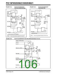
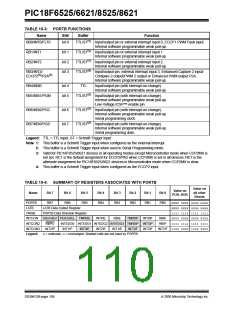
TABLE 10-3: PORTB FUNCTIONS
Name
Bit#
Buffer
Function
RB0/INT0/FLT0
bit 0
TTL/ST(1) Input/output pin or external interrupt input 0, ECCP1 PWM Fault input.
Internal software programmable weak pull-up.
RB1/INT1
RB2/INT2
bit 1
bit 2
bit 3
TTL/ST(1) Input/output pin or external interrupt input 1.
Internal software programmable weak pull-up.
TTL/ST(1) Input/output pin or external interrupt input 2.
Internal software programmable weak pull-up.
TTL/ST(4) Input/output pin, external interrupt input 3, Enhanced Capture 2 input/
Compare 2 output/PWM 2 output or Enhanced PWM output P2A.
Internal software programmable weak pull-up.
RB3/INT3/
ECCP2(3)/P2A(3)
RB4/KBI0
bit 4
bit 5
TTL
Input/output pin (with interrupt-on-change).
Internal software programmable weak pull-up.
RB5/KBI1/PGM
TTL/ST(2) Input/output pin (with interrupt-on-change).
Internal software programmable weak pull-up.
Low-Voltage ICSP™ enable pin.
RB6/KBI2/PGC
RB7/KBI3/PGD
bit 6
bit 7
TTL/ST(2) Input/output pin (with interrupt-on-change).
Internal software programmable weak pull-up.
Serial programming clock.
TTL/ST(2) Input/output pin (with interrupt-on-change).
Internal software programmable weak pull-up.
Serial programming data.
Legend: TTL = TTL input, ST = Schmitt Trigger input
Note 1: This buffer is a Schmitt Trigger input when configured as the external interrupt.
2: This buffer is a Schmitt Trigger input when used in Serial Programming mode.
3: Valid for PIC18F8525/8621 devices in all operating modes except Microcontroller mode when CCP2MX is
not set. RC1 is the default assignment for ECCP2/PA2 when CCP2MX is set in all devices; RE7 is the
alternate assignment for PIC18F8525/8621 devices in Microcontroller mode when CCP2MX is clear.
4: This buffer is a Schmitt Trigger input when configured as the ECCP2 input.
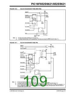
TABLE 10-4: SUMMARY OF REGISTERS ASSOCIATED WITH PORTB
Value on
Value on
POR, BOR
Name
Bit 7
Bit 6
Bit 5
Bit 4
Bit 3
Bit 2
Bit 1
Bit 0
all other
Resets
PORTB
LATB
RB7
RB6
RB5
RB4
RB3
RB2
RB1
RB0
xxxx xxxx uuuu uuuu
xxxx xxxx uuuu uuuu
1111 1111 1111 1111
0000 000x 0000 000u
1111 1111 1111 1111
LATB Data Output Register
TRISB
PORTB Data Direction Register
GIE/GIEH PEIE/GIEL TMR0IE
INTCON
INTCON2
INTCON3
Legend:
INT0IE
RBIE
TMR0IF INT0IF
RBIF
RBIP
RBPU
INTEDG0 INTEDG1 INTEDG2 INTEDG3 TMR0IP INT3IP
INT1IP INT3IE INT2IE INT1IE INT3IF INT2IF
INT2IP
INT1IF 1100 0000 1100 0000
x= unknown, u= unchanged. Shaded cells are not used by PORTB.
DS39612B-page 108
2005 Microchip Technology Inc.

 MICROCHIP [ MICROCHIP ]