PIC18F6525/6621/8525/8621
When the Parallel Slave Port is active, three PORTE
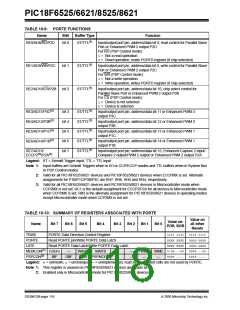
10.5 PORTE, TRISE and LATE
Registers
pins (RE0/AD8/RD/P2D, RE1/AD9/WR/P2C and RE2/
AD10/CS/P2B) function as its control inputs. This
automatically occurs when the PSPMODE bit
(PSPCON<4>) is set. Users must also make certain
that bits TRISE<2:0> are set to configure the pins as
digital inputs and the ADCON1 register is configured
for digital I/O. The PORTE PSP control functions are
summarized in Table 10-9.
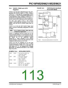
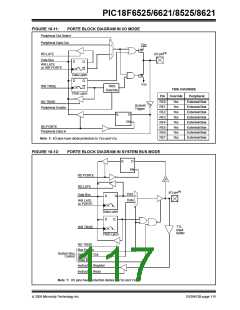
PORTE is an 8-bit wide, bidirectional port. The corre-
sponding data direction register is TRISE. Setting a
TRISE bit (= 1) will make the corresponding PORTE
pin an input (i.e., put the corresponding output driver in
a high-impedance mode). Clearing a TRISE bit (= 0)
will make the corresponding PORTE pin an output (i.e.,
put the contents of the output latch on the selected pin).
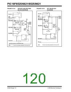
Pin RE7 can be configured as the alternate peripheral
pin for the ECCP2 module when the device is operating
in Microcontroller mode. This is done by clearing the
configuration bit, CCP2MX, in the CONFIG3H
Configuration register (CONFIG3H<0>).
Read-modify-write operations on the LATE register,
read and write the latched output value for PORTE.
PORTE is an 8-bit port with Schmitt Trigger input
buffers. Each pin is individually configurable as an input
or output. PORTE is multiplexed with the ECCP
module (Table 10-9).
Note:
For PIC18F8525/8621 (80-pin) devices
operating in Extended Microcontroller
mode, PORTE defaults to the system bus
on Power-on Reset.
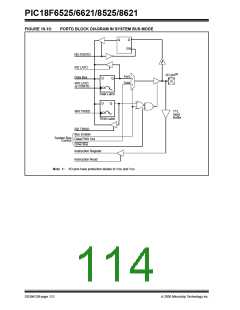
On PIC18F8525/8621 devices, PORTE is also
multiplexed with the system bus as the external memory
interface; the I/O bus is available only when the system
bus is disabled by setting the EBDIS bit in the MEMCON
register (MEMCON<7>). If the device is configured in
Microprocessor or Extended Microcontroller mode, then
the PORTE<7:0> becomes the high byte of the address/
data bus for the external program memory interface. In
Microcontroller mode, the PORTE<2:0> pins become
the control inputs for the Parallel Slave Port when bit
PSPMODE (PSPCON<4>) is set. (Refer to
Section 4.1.1 “PIC18F6525/6621/8525/8621 Program
Memory Modes” for more information.)
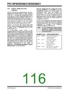
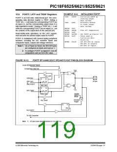
EXAMPLE 10-5:
INITIALIZING PORTE
CLRF
PORTE
; Initialize PORTE by
; clearing output
; data latches
CLRF
LATE
; Alternate method
; to clear output
; data latches
MOVLW
MOVWF
0x03
; Value used to
;initializedata
; direction
; Set RE1:RE0 as inputs
; RE7:RE2 as outputs
TRISE
DS39612B-page 114
2005 Microchip Technology Inc.

 MICROCHIP [ MICROCHIP ]