PIC18F6525/6621/8525/8621
The pin override value is not loaded into the TRIS
register. This allows read-modify-write of the TRIS
register without concern due to peripheral overrides.
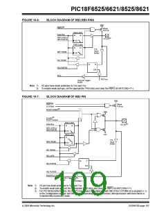
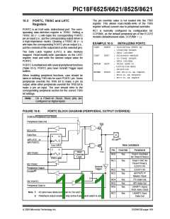
10.3 PORTC, TRISC and LATC
Registers
PORTC is an 8-bit wide, bidirectional port. The corre-
sponding data direction register is TRISC. Setting a
TRISC bit (= 1) will make the corresponding PORTC
pin an input (i.e., put the corresponding output driver in
a high-impedance mode). Clearing a TRISC bit (= 0)
will make the corresponding PORTC pin an output (i.e.,
put the contents of the output latch on the selected pin).
RC1 is normally configured by configuration bit,
CCP2MX, as the default peripheral pin of the ECCP2
module (default/erased state, CCP2MX = 1).
EXAMPLE 10-3:
INITIALIZING PORTC
CLRF
PORTC
; Initialize PORTC by
; clearing output
; data latches
The Data Latch register (LATC) is also memory
mapped. Read-modify-write operations on the LATC
register, read and write the latched output value for
PORTC.
CLRF
LATC
; Alternate method
; to clear output
; data latches
MOVLW
MOVWF
0xCF
; Value used to
; initialize data
; direction
; Set RC<3:0> as inputs
; RC<5:4> as outputs
; RC<7:6> as inputs
PORTC is multiplexed with several peripheral functions
(Table 10-5). PORTC pins have Schmitt Trigger input
buffers.
TRISC
When enabling peripheral functions, care should be
taken in defining TRIS bits for each PORTC pin. Some
peripherals override the TRIS bit to make a pin an
output, while other peripherals override the TRIS bit to
make a pin an input. The user should refer to the
corresponding peripheral section for the correct TRIS
bit settings.
Note:
On a Power-on Reset, these pins are
configured as digital inputs.
FIGURE 10-8:
PORTC BLOCK DIAGRAM (PERIPHERAL OUTPUT OVERRIDE)
PORTC/Peripheral Out Select
Peripheral Data Out
VDD
P
0
1
RD LATC
Data Bus
D
Q
Q
(1)
I/O pin
or
WR LATC
CK
WR PORTC
Data Latch
TRIS OVERRIDE
N
D
Q
Q
Pin
Override
Peripheral
VSS
TRIS
Override
Logic
WR TRISC
CK
RC0
Yes
Timer1 Oscillator
for Timer1/Timer3
TRIS Latch
RC1
Yes
Timer1 OSC for
Timer1/Timer3,
ECCP2 I/O
RD TRISC
Schmitt
Trigger
Peripheral Output
RC2
RC3
Yes
Yes
ECCP1 I/O
(2)
Enable
2
Q
D
SPI™/I C™
Master Clock
EN
2
RC4
RC5
RC6
Yes
Yes
Yes
I C Data Out
RD PORTC
SPI Data Out
Peripheral Data In
USART1 Async
Xmit, Sync Clock
Note 1: I/O pins have diode protection to VDD and VSS.
2: Peripheral output enable is only active if peripheral select is active.
RC7
Yes
USART1 Sync
Data Out
2005 Microchip Technology Inc.
DS39612B-page 109

 MICROCHIP [ MICROCHIP ]