PIC18F6525/6621/8525/8621
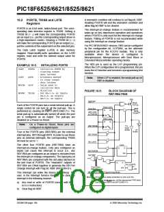
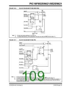
FIGURE 10-6:
BLOCK DIAGRAM OF RB2:RB0 PINS
VDD
RBPU(2)
Weak
P
Pull-up
Data Latch
Data Bus
D
Q
WR LATB or
WR PORTB
I/O pin(1)
CK
TRIS Latch
D
Q
TTL
Input
Buffer
WR TRISB
CK
RD TRISB
Q
D
RD PORTB
EN
INTx
RD Port
Schmitt Trigger
Buffer
Note 1: I/O pins have diode protection to VDD and VSS.
2: To enable weak pull-ups, set the appropriate TRIS bit(s) and clear the RBPU bit (INTCON2<7>).
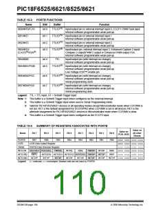
FIGURE 10-7:
BLOCK DIAGRAM OF RB3 PIN
VDD
Weak
RBPU(2)
CCP2MX
P
Pull-up
ECCP Output(3)
1
VDD
P
Enable(3)
ECCP Output
0
Data Latch
Data Bus
I/O pin(1)
D
Q
WR LATB or
WR PORTB
N
CK
VSS
TRIS Latch
D
TTL
WR TRISB
Input
CK
Q
Buffer
RD TRISB
RD LATB
D
Q
RD PORTB
EN
RD PORTB
ECCP2 or INT3
Schmitt Trigger
Buffer
CCP2MX = 0
Note 1: I/O pin has diode protection to VDD and VSS.
2: To enable weak pull-ups, set the appropriate TRIS bit(s) and clear the RBPU bit (INTCON2<7>).
3: For PIC18F8525/8621 parts, the ECCP2 input/output is multiplexed with RB3 if the CCP2MX bit is enabled (= 0)
in the Configuration register and the device is operating in Microprocessor, Microprocessor with Boot Block or
Extended Microcontroller mode.
2005 Microchip Technology Inc.
DS39612B-page 107

 MICROCHIP [ MICROCHIP ]