PIC18F6525/6621/8525/8621
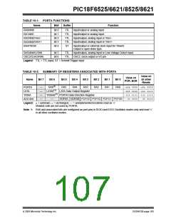
TABLE 10-1: PORTA FUNCTIONS
Name
RA0/AN0
Bit#
Buffer
Function
bit 0
bit 1
bit 2
bit 3
bit 4
TTL
TTL
TTL
TTL
ST
Input/output or analog input.
RA1/AN1
Input/output or analog input.
RA2/AN2/VREF-
RA3/AN3/VREF+
RA4/T0CKI
Input/output, analog input or VREF-.
Input/output, analog input or VREF+.
Input/output or external clock input for Timer0.
Output is open-drain type.
RA5/AN4/LVDIN
OSC2/CLKO/RA6
bit 5
bit 6
TTL
TTL
Input/output, analog input or Low-Voltage Detect input.
OSC2, clock output or I/O pin
Legend: TTL = TTL input, ST = Schmitt Trigger input
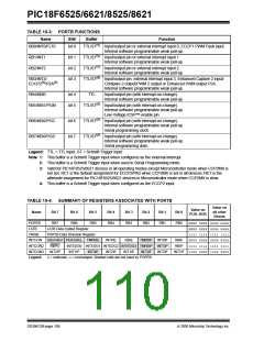
TABLE 10-2: SUMMARY OF REGISTERS ASSOCIATED WITH PORTA
Value on
all other
Resets
Value on
POR, BOR
Name
Bit 7
Bit 6
Bit 5
Bit 4
Bit 3
Bit 2
Bit 1
Bit 0
PORTA
LATA
—
—
—
—
RA6(1)
RA5
RA4
RA3
RA2
RA1
RA0
-x0x 0000 -u0u 0000
-xxx xxxx -uuu uuuu
-111 1111 -111 1111
LATA6(1) LATA Data Output Register
TRISA6(1) PORTA Data Direction Register
TRISA
ADCON1
—
VCFG1 VCFG0 PCFG3 PCFG2 PCFG1 PCFG0 --00 0000 --00 0000
Legend: x= unknown, u= unchanged, — = unimplemented locations read as ‘0’.
Shaded cells are not used by PORTA.
Note 1: RA6 and associated bits are configured as port pins in RCIO and ECIO Oscillator modes only and read ‘0’
in all other oscillator modes.
2005 Microchip Technology Inc.
DS39612B-page 105

 MICROCHIP [ MICROCHIP ]