PIC17C4X
12.2.3 EXTERNAL CLOCK INPUT FOR TIMER3
EXAMPLE 12-2: WRITING TO TMR3
BSF
CPUSTA, GLINTD ;Disable interrupt
When TMR3CS is set, the 16-bit TMR3 increments on
the falling edge of clock input TCLK3. The input on the
RB5/TCLK3 pin is sampled and synchronized by the
internal phase clocks twice every instruction cycle.This
causes a delay from the time a falling edge appears on
TCLK3 to the time TMR3 is actually incremented. For
the external clock input timing requirements, see the
Electrical Specification section. Figure 12-9 shows the
timing diagram when operating from an external clock.
MOVFP RAM_L, TMR3L
MOVFP RAM_H, TMR3H
BCF
;
;
CPUSTA, GLINTD ;Done,enable interrupt
EXAMPLE 12-3: READING FROM TMR3
MOVPF
MOVPF
MOVFP
CPFSLT TMR3L, WREG
RETURN
MOVPF
MOVPF
RETURN
TMR3L, TMPLO
TMR3H, TMPHI
TMPLO, WREG
;read low tmr0
;read high tmr0
;tmplo −> wreg
;tmr0l < wreg?
;no then return
;read low tmr0
;read high tmr0
;return
12.2.4 READING/WRITING TIMER3
TMR3L, TMPLO
TMR3H, TMPHI
Since Timer3 is a 16-bit timer and only 8-bits at a time
can be read or written, care should be taken when
reading or writing while the timer is running. The best
method to read or write the timer is to stop the timer,
perform any read or write operation, and then restart
Timer3 (using the TMR3ON bit). However, if it is neces-
sary to keep Timer3 free-running, care must be taken.
For writing to the 16-bit TMR3, Example 12-2 may be
used. For reading the 16-bit TMR3, Example 12-3 may
be used. Interrupts must be disabled during this rou-
tine.
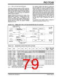
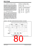
FIGURE 12-9: TMR1,TMR2, AND TMR3 OPERATION IN EXTERNAL CLOCK MODE
Q1 Q2 Q3 Q4 Q1 Q2 Q3 Q4 Q1 Q2 Q3 Q4 Q1 Q2 Q3 Q4 Q1 Q2 Q3 Q4 Q1 Q2 Q3 Q4
TCLK12
34h
35h
A8h
A9h
00h
TMR1, TMR2, or TMR3
PR1, PR2, or PR3H:PR3L
WR_TMR
'A9h'
'A9h'
Read_TMR
TMRxIF
MOVWF
TMRx
MOVFP
MOVFP
TMRx,W
TMRx,W
Instruction
executed
Write to TMRx
Read TMRx
Read TMRx
Note 1: TCLK12 is sampled in Q2 and Q4.
2: ↓ indicates a sampling point.
3: The latency from TCLK12 ↓ to timer increment is between 2Tosc and 6Tosc.
DS30412C-page 80
1996 Microchip Technology Inc.

 MICROCHIP [ MICROCHIP ]