PIC17C4X
12.1.3.1 PWM PERIODS
The user should also avoid any "read-modify-write"
operations on the duty cycle registers, such as:ADDWF
PW1DCH. This may cause duty cycle outputs that are
unpredictable.
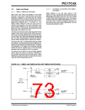
The period of the PWM1 output is determined by
Timer1 and its period register (PR1). The period of the
PWM2 output can be software configured to use either
Timer1 or Timer2 as the time-base. When TM2PW2 bit
(PW2DCL<5>) is clear, the time-base is determined by
TMR1 and PR1. When TM2PW2 is set, the time-base
is determined by Timer2 and PR2.
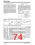
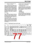
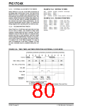
TABLE 12-3: PWM FREQUENCY vs.
RESOLUTION AT 25 MHz
Frequency (kHz)
PWM
Running two different PWM outputs on two different
timers allows different PWM periods. Running both
PWMs from Timer1 allows the best use of resources by
freeing Timer2 to operate as an 8-bit timer. Timer1 and
Timer2 can not be used as a 16-bit timer if either PWM
is being used.
Frequency
24.4 48.8 65.104 97.66 390.6
PRx Value 0xFF 0x7F 0x5F
0x3F
0x0F
6-bit
High
Resolution
10-bit 9-bit 8.5-bit 8-bit
Standard
8-bit
7-bit 6.5-bit 6-bit
4-bit
The PWM periods can be calculated as follows:
period of PWM1 =[(PR1) + 1] x 4TOSC
Resolution
12.1.3.2 PWM INTERRUPTS
period of PWM2 =[(PR1) + 1] x 4TOSC or
[(PR2) + 1] x 4TOSC
The PWM module makes use of TMR1 or TMR2 inter-
rupts. A timer interrupt is generated when TMR1 or
TMR2 equals its period register and is cleared to zero.
This interrupt also marks the beginning of a PWM
cycle. The user can write new duty cycle values before
the timer roll-over. The TMR1 interrupt is latched into
the TMR1IF bit and the TMR2 interrupt is latched into
the TMR2IF bit. These flags must be cleared in soft-
ware.
The duty cycle of PWMx is determined by the 10-bit
value DCx<9:0>. The upper 8-bits are from register
PWxDCH and the lower 2-bits are from PWxDCL<7:6>
(PWxDCH:PWxDCL<7:6>). Table 12-3 shows the
maximum PWM frequency (FPWM) given the value in
the period register.
The number of bits of resolution that the PWM can
achieve depends on the operation frequency of the
device as well as the PWM frequency (FPWM).
12.1.3.3 EXTERNAL CLOCK SOURCE
Maximum PWM resolution (bits) for a given PWM fre-
quency:
The PWMs will operate regardless of the clock source
of the timer. The use of an external clock has ramifica-
tions that must be understood. Because the external
TCLK12 input is synchronized internally (sampled once
per instruction cycle), the time TCLK12 changes to the
time the timer increments will vary by as much as TCY
(one instruction cycle). This will cause jitter in the duty
cycle as well as the period of the PWM output.
FOSC
log ( FPWM )
=
bits
log (2)
The PWMx duty cycle is as follows:
This jitter will be ±TCY, unless the external clock is syn-
chronized with the processor clock. Use of one of the
PWM outputs as the clock source to the TCLKx input,
will supply a synchronized clock.
PWMx Duty Cycle = (DCx) x TOSC
where DCx represents the 10-bit value from
PWxDCH:PWxDCL.
If DCx = 0, then the duty cycle is zero. If PRx =
PWxDCH, then the PWM output will be low for one to
four Q-clock (depending on the state of the
PWxDCL<7:6> bits). For a Duty Cycle to be 100%, the
PWxDCH value must be greater then the PRx value.
In general, when using an external clock source for
PWM, its frequency should be much less than the
device frequency (Fosc).
The duty cycle registers for both PWM outputs are dou-
ble buffered. When the user writes to these registers,
they are stored in master latches. When TMR1 (or
TMR2) overflows and a new PWM period begins, the
master latch values are transferred to the slave latches
and the PWMx pin is forced high.
Note: For PW1DCH, PW1DCL, PW2DCH and
PW2DCL registers,
a write operation
writes to the "master latches" while a read
operation reads the "slave latches". As a
result, the user may not read back what
was just written to the duty cycle registers.
DS30412C-page 76
1996 Microchip Technology Inc.

 MICROCHIP [ MICROCHIP ]