PIC17C4X
12.2.2 DUAL CAPTURE REGISTER MODE
The Capture2 overflow status flag bit is double buff-
ered. The master bit is set if one captured word is
already residing in the Capture2 register and another
“event” has occurred on the RB1/CA2 pin. The new
event will not transfer the TMR3 value to the capture
register which protects the previous unread capture
value. When the user reads both the high and the low
bytes (in any order) of the Capture2 register, the master
overflow bit is transferred to the slave overflow bit
(CA2OVF) and then the master bit is reset. The user
can then read TCON2 to determine the value of
CA2OVF.
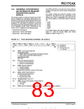
This mode is selected by setting CA1/PR3. A block dia-
gram is shown in Figure 12-8. In this mode, TMR3 runs
without a period register and increments from 0000h to
FFFFh and rolls over to 0000h. The TMR3 interrupt
Flag (TMR3IF) is set on this roll over. The TMR3IF bit
must be cleared in software.
Registers PR3H/CA1H and PR3L/CA1L make a 16-bit
capture register (Capture1). It captures events on pin
RB0/CAP1. Capture mode is configured by the
CA1ED1 and CA1ED0 bits. Capture1 Interrupt Flag bit
(CA1IF) is set on the capture event.The corresponding
interrupt mask bit is CA1IE. The Capture1 Overflow
Status bit is CA1OVF.
The operation of the Capture1 feature is identical to
Capture2 (as described in Section 12.2.1).
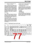
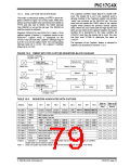
FIGURE 12-8: TIMER3 WITH TWO CAPTURE REGISTERS BLOCK DIAGRAM
CA1ED1, CA1ED0
(TCON1<5:4>)
2
Set CA1IF
(PIR<2>)
PR3H/CA1H
Capture Enable
PR3L/CA1L
TMR3L
Edge Select
Prescaler Select
RB0/CAP1
Set TMR3IF
(PIR<6>)
Fosc/4
0
1
TMR3H
TMR3ON
(TCON2<2>)
RB5/TCLK3
RB1/CAP2
Capture Enable
TMR3CS
(TCON1<2>)
Edge Select
Set CA2IF
(PIR<3>)
Prescaler Select
CA2H
CA2L
2
CA2ED1, CA2ED0
(TCON1<7:6>)
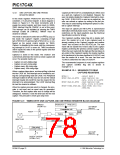
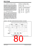
TABLE 12-5: REGISTERS ASSOCIATED WITH CAPTURE
Value on
Value on all
Address
Name
Bit 7
Bit 6
Bit 5
Bit 4
Bit 3
Bit 2
Bit 1
Bit 0
Power-on other resets
Reset (Note1)
16h, Bank 3
17h, Bank 3
12h, Bank 2
13h, Bank 2
16h, Bank 1
17h, Bank 1
TCON1
TCON2
TMR3L
TMR3H
PIR
CA2ED1 CA2ED0 CA1ED1
CA1ED0
T16
TMR3CS TMR2CS TMR1CS 0000 0000 0000 0000
CA2OVF CA1OVF PWM2ON PWM1ON CA1/PR3 TMR3ON TMR2ON TMR1ON 0000 0000 0000 0000
TMR3 register; low byte
TMR3 register; high byte
xxxx xxxx uuuu uuuu
xxxx xxxx uuuu uuuu
0000 0010 0000 0010
0000 0000 0000 0000
0000 0000 0000 0000
--11 11-- --11 qq--
xxxx xxxx uuuu uuuu
xxxx xxxx uuuu uuuu
xxxx xxxx uuuu uuuu
xxxx xxxx uuuu uuuu
RBIF
RBIE
PEIF
—
TMR3IF
TMR3IE
T0CKIF
—
TMR2IF
TMR2IE
T0IF
TMR1IF
TMR1IE
INTF
CA2IF
CA2IE
PEIE
TO
CA1IF
CA1IE
T0CKIE
PD
TXIF
TXIE
T0IE
—
RCIF
RCIE
INTE
—
PIE
07h, Unbanked INTSTA
06h, Unbanked CPUSTA
STKAV
GLINTD
16h, Bank 2
17h, Bank 2
14h, Bank 3
15h, Bank 3
PR3L/CA1L Timer3 period register, low byte/capture1 register, low byte
PR3H/CA1H Timer3 period register, high byte/capture1 register, high byte
CA2L
CA2H
Capture2 low byte
Capture2 high byte
Legend: x= unknown, u= unchanged, -= unimplemented read as '0', q- value depends on condition,
shaded cells are not used by Capture.
Note 1: Other (non power-up) resets include: external reset through MCLR and WDT Timer Reset.
1996 Microchip Technology Inc.
DS30412C-page 79

 MICROCHIP [ MICROCHIP ]