PIC17C4X
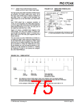
12.1.3.3.1 MAX RESOLUTION/FREQUENCY FOR
EXTERNAL CLOCK INPUT
Timer3 has two modes of operation, depending on the
CA1/PR3 bit (TCON2<3>). These modes are:
• One capture and one period register mode
• Dual capture register mode
The use of an external clock for the PWM time-base
(Timer1 or Timer2) limits the PWM output to a maxi-
mum resolution of 8-bits. The PWxDCL<7:6> bits must
be kept cleared. Use of any other value will distort the
PWM output. All resolutions are supported when inter-
nal clock mode is selected. The maximum attainable
frequency is also lower. This is a result of the timing
requirements of an external clock input for a timer (see
the Electrical Specification section). The maximum
PWM frequency, when the timers clock source is the
RB4/TCLK12 pin, is shown in Table 12-3 (standard res-
olution mode).
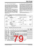
The PIC17C4X has up to two 16-bit capture registers
that capture the 16-bit value of TMR3 when events are
detected on capture pins. There are two capture pins
(RB0/CAP1 and RB1/CAP2), one for each capture reg-
ister. The capture pins are multiplexed with PORTB
pins. An event can be:
• a rising edge
• a falling edge
• every 4th rising edge
• every 16th rising edge
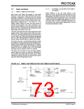
12.2
Timer3
Each 16-bit capture register has an interrupt flag asso-
ciated with it. The flag is set when a capture is made.
The capture module is truly part of the Timer3 block.
Figure 12-7 and Figure 12-8 show the block diagrams
for the two modes of operation.
Timer3 is a 16-bit timer consisting of the TMR3H and
TMR3L registers. TMR3H is the high byte of the timer
and TMR3L is the low byte. This timer has an associ-
ated 16-bit period register (PR3H/CA1H:PR3L/CA1L).
This period register can be software configured to be a
second 16-bit capture register.
When the TMR3CS bit (TCON1<2>) is clear, the timer
increments every instruction cycle (Fosc/4). When
TMR3CS is set, the timer increments on every falling
edge of the RB5/TCLK3 pin. In either mode, the
TMR3ON bit must be set for the timer to increment.
When TMR3ON is clear, the timer will not increment or
set the TMR3IF bit.
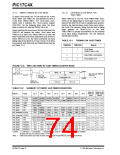
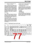
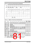
TABLE 12-4: REGISTERS/BITS ASSOCIATED WITH PWM
Value on all
other
resets
Value on
Power-on
Reset
Address
Name
Bit 7
Bit 6
Bit 5
Bit 4
Bit 3
Bit 2
Bit 1
Bit 0
(Note1)
16h, Bank 3
TCON1
CA2ED1
CA2OVF
CA2ED0
CA1ED1
CA1ED0
T16
TMR3CS TMR2CS TMR1CS 0000 0000 0000 0000
17h, Bank 3
10h, Bank 2
11h, Bank 2
16h, Bank 1
17h, Bank 1
TCON2
TMR1
TMR2
PIR
CA1OVF PWM2ON PWM1ON CA1/PR3 TMR3ON TMR2ON TMR1ON 0000 0000 0000 0000
Timer1 register
Timer2 register
xxxx xxxx uuuu uuuu
xxxx xxxx uuuu uuuu
0000 0010 0000 0010
0000 0000 0000 0000
0000 0000 0000 0000
RBIF
RBIE
PEIF
TMR3IF
TMR2IF
TMR2IE
T0IF
TMR1IF
TMR1IE
INTF
CA2IF
CA2IE
PEIE
CA1IF
CA1IE
TXIF
TXIE
T0IE
RCIF
RCIE
INTE
PIE
TMR3IE
T0CKIF
07h, Unbanked INTSTA
06h, Unbanked CPUSTA
T0CKIE
—
—
STKAV
—
GLINTD
—
TO
—
PD
—
—
—
—
—
--11 11-- --11 qq--
xx-- ---- uu-- ----
xx0- ---- uu0- ----
xxxx xxxx uuuu uuuu
xxxx xxxx uuuu uuuu
10h, Bank 3
11h, Bank 3
12h, Bank 3
13h, Bank 3
PW1DCL
PW2DCL
PW1DCH
PW2DCH
DC1
DC1
DC9
DC9
DC0
DC0
DC8
DC8
TM2PW2
DC7
—
—
—
—
—
DC6
DC6
DC5
DC5
DC4
DC4
DC3
DC3
DC2
DC2
DC7
Legend: x= unknown, u= unchanged, -= unimplemented read as '0', q= value depends on conditions,
shaded cells are not used by PWM.
1996 Microchip Technology Inc.
DS30412C-page 77

 MICROCHIP [ MICROCHIP ]