PIC17C4X
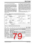
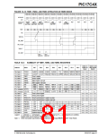
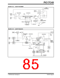
FIGURE 12-10: TMR1,TMR2, AND TMR3 OPERATION IN TIMER MODE
Q1Q2Q3Q4 Q1Q2Q3Q4 Q1Q2Q3Q4 Q1Q2Q3Q4 Q1Q2Q3Q4 Q1Q2Q3Q4 Q1Q2Q3Q4 Q1Q2Q3Q4 Q1Q2Q3Q4 Q1Q2Q3Q4 Q1Q2Q3Q4
AD15:AD0
ALE
BCF
TCON2, 0
Start TMR1
MOVF
BSF
MOVWF
TMR1
MOVF
NOP
07h
NOP
NOP
NOP
00h
Instruction
fetched
MOVLB 3
NOP
06h
TMR1, W
Read TMR1
TCON2, 0
Stop TMR1
TMR1, W
Write TMR1 Read TMR1
TMR1
PR1
04h
05h
03h
04h
05h
08h
TMR1ON
WR_TMR1
WR_TCON2
TMR1IF
RD_TMR1
TMR1
reads 03h
TMR1
reads 04h
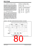
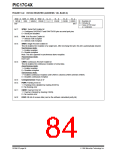
TABLE 12-6: SUMMARY OF TMR1,TMR2, AND TMR3 REGISTERS
Value on
Value on all
Address
Name
Bit 7
Bit 6
Bit 5
Bit 4
Bit 3
Bit 2
Bit 1
Bit 0
Power-on other resets
Reset (Note1)
16h, Bank 3
TCON1
CA2ED1 CA2ED0 CA1ED1 CA1ED0
T16
TMR3CS TMR2CS TMR1CS 0000 0000 0000 0000
17h, Bank 3
10h, Bank 2
11h, Bank 2
12h, Bank 2
13h, Bank 2
16h, Bank 1
17h, Bank 1
TCON2
TMR1
TMR2
TMR3L
TMR3H
PIR
CA2OVF CA1OVF PWM2ON PWM1ON CA1/PR3 TMR3ON TMR2ON TMR1ON 0000 0000 0000 0000
Timer1 register
xxxx xxxx uuuu uuuu
xxxx xxxx uuuu uuuu
xxxx xxxx uuuu uuuu
xxxx xxxx uuuu uuuu
0000 0010 0000 0010
0000 0000 0000 0000
0000 0000 0000 0000
Timer2 register
TMR3 register; low byte
TMR3 register; high byte
RBIF
RBIE
PEIF
TMR3IF
TMR2IF
TMR1IF
TMR1IE
INTF
CA2IF
CA2IE
PEIE
CA1IF
CA1IE
TXIF
TXIE
T0IE
RCIF
RCIE
INTE
PIE
TMR3IE TMR2IE
07h, Unbanked INTSTA
06h, Unbanked CPUSTA
T0CKIF
—
T0IF
T0CKIE
—
STKAV
GLINTD
TO
PD
—
—
--11 11-- --11 qq--
xxxx xxxx uuuu uuuu
xxxx xxxx uuuu uuuu
xxxx xxxx uuuu uuuu
xxxx xxxx uuuu uuuu
xx-- ---- uu-- ----
xx0- ---- uu0- ----
xxxx xxxx uuuu uuuu
xxxx xxxx uuuu uuuu
xxxx xxxx uuuu uuuu
xxxx xxxx uuuu uuuu
14h, Bank 2
15h, Bank 2
16h, Bank 2
17h, Bank 2
10h, Bank 3
11h, Bank 3
12h, Bank 3
13h, Bank 3
14h, Bank 3
15h, Bank 3
PR1
PR2
Timer1 period register
Timer2 period register
PR3L/CA1L Timer3 period/capture1 register; low byte
PR3H/CA1H Timer3 period/capture1 register; high byte
PW1DCL
PW2DCL
PW1DCH
PW2DCH
CA2L
DC1
DC1
DC9
DC9
DC0
DC0
DC8
DC8
—
TM2PW2
DC7
—
—
—
—
—
—
—
—
—
—
DC6
DC6
DC5
DC5
DC4
DC4
DC3
DC3
DC2
DC2
DC7
Capture2 low byte
Capture2 high byte
CA2H
Legend: x= unknown, u= unchanged, -= unimplemented read as '0', q- value depends on condition,
shaded cells are not used by TMR1, TMR2 or TMR3.
Note 1: Other (non power-up) resets include: external reset through MCLR and WDT Timer Reset.
1996 Microchip Technology Inc.
DS30412C-page 81

 MICROCHIP [ MICROCHIP ]