PIC17C4X
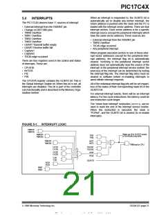
When an interrupt is responded to, the GLINTD bit is
automatically set to disable any further interrupt, the
return address is pushed onto the stack and the PC is
loaded with the interrupt vector address.There are four
interrupt vectors. Each vector address is for a specific
interrupt source (except the peripheral interrupts which
have the same vector address). These sources are:
5.0
INTERRUPTS
The PIC17C4X devices have 11 sources of interrupt:
• External interrupt from the RA0/INT pin
• Change on RB7:RB0 pins
• TMR0 Overflow
• TMR1 Overflow
• TMR2 Overflow
• TMR3 Overflow
• USART Transmit buffer empty
• USART Receive buffer full
• Capture1
• External interrupt from the RA0/INT pin
• TMR0 Overflow
• T0CKI edge occurred
• Any peripheral interrupt
When program execution vectors to one of these inter-
rupt vector addresses (except for the peripheral inter-
rupt address), the interrupt flag bit is automatically
cleared. Vectoring to the peripheral interrupt vector
address does not automatically clear the source of the
interrupt. In the peripheral interrupt service routine, the
source(s) of the interrupt can be determined by testing
the interrupt flag bits. The interrupt flag bit(s) must be
cleared in software before re-enabling interrupts to
avoid infinite interrupt requests.
• Capture2
• T0CKI edge occurred
There are four registers used in the control and status
of interrupts. These are:
• CPUSTA
• INTSTA
• PIE
• PIR
The CPUSTA register contains the GLINTD bit. This is
the Global Interrupt Disable bit. When this bit is set, all
interrupts are disabled. This bit is part of the controller
core functionality and is described in the Memory Orga-
nization section.
All of the individual interrupt flag bits will be set regard-
less of the status of their corresponding mask bit or the
GLINTD bit.
For external interrupt events, there will be an interrupt
latency. For two cycle instructions, the latency could be
one instruction cycle longer.
The “return from interrupt” instruction, RETFIE, can be
used to mark the end of the interrupt service routine.
When this instruction is executed, the stack is
“POPed”, and the GLINTD bit is cleared (to re-enable
interrupts).
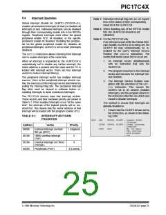
FIGURE 5-1: INTERRUPT LOGIC
TMR1IF
TMR1IE
Wake-up (If in SLEEP mode)
or terminate long write
TMR2IF
TMR2IE
T0IF
T0IE
TMR3IF
TMR3IE
INTF
INTE
Interrupt to CPU
CA1IF
CA1IE
T0CKIF
T0CKIE
CA2IF
CA2IE
PEIF
PEIE
TXIF
TXIE
GLINTD
RCIF
RCIE
RBIF
RBIE
1996 Microchip Technology Inc.
DS30412C-page 21
This document was created with FrameMaker 4 0 4

 MICROCHIP [ MICROCHIP ]