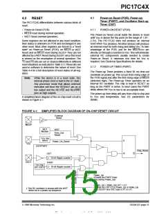
PIC17C4X
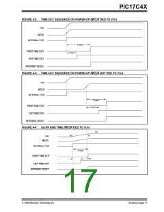
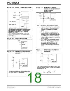
FIGURE 4-5: OSCILLATORSTART-UPTIME
FIGURE 4-8: PIC17C42 EXTERNAL
POWER-ON RESET CIRCUIT
(FOR SLOW VDD
POWER-UP)
VDD
VDD
VDD
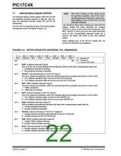
MCLR
OSC2
D
R
R1
MCLR
TOSC1
TOST
PIC17C42
C
OST TIME_OUT
PWRT TIME_OUT
Note 1: An external Power-on Reset circuit is
required only if VDD power-up time is too
slow. The diode D helps discharge the
capacitor quickly when VDD powers
down.
TPWRT
INTERNAL RESET
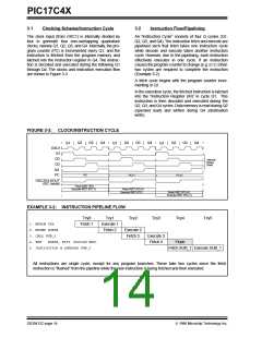
This figure shows in greater detail the timings involved
with the oscillator start-up timer. In this example the
low frequency crystal start-up time is larger than
power-up time (TPWRT).
Tosc1 = time for the crystal oscillator to react to an
oscillation level detectable by the Oscillator Start-up
Timer (ost).
2: R < 40 kΩ is recommended to ensure
that the voltage drop across R does not
exceed 0.2V (max. leakage current spec.
on the MCLR/VPP pin is 5 µA). A larger
voltage drop will degrade VIH level on the
MCLR/VPP pin.
TOST = 1024TOSC.
FIGURE 4-6: USING ON-CHIP POR
3: R1 = 100Ω to 1 kΩ will limit any current
flowing into MCLR from external capaci-
tor C in the event of MCLR/VPP pin
breakdown due to Electrostatic Dis-
charge (ESD) or (Electrical Overstress)
EOS.
VDD
VDD
MCLR
PIC17CXX
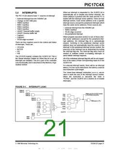
FIGURE 4-9: BROWN-OUT PROTECTION
CIRCUIT 2
FIGURE 4-7: BROWN-OUT PROTECTION
CIRCUIT 1
VDD
VDD
R1
VDD
Q1
VDD
MCLR
33k
R2
40 kΩ
PIC17CXX
10k
MCLR
40 kΩ
PIC17CXX
This brown-out circuit is less expensive, albeit less
accurate. Transistor Q1 turns off when VDD is below a
certain level such that:
R1
This circuit will activate reset when VDD goes below
(Vz + 0.7V) where Vz = Zener voltage.
= 0.7V
VDD •
R1 + R2
DS30412C-page 18
1996 Microchip Technology Inc.

 MICROCHIP [ MICROCHIP ]