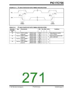
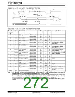
PIC17C75X
2
E.2
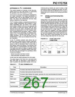
ADDRESSING I C DEVICES
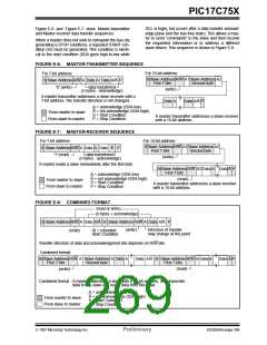
FIGURE E-4: SLAVE-RECEIVER
ACKNOWLEDGE
There are two address formats. The simplest is the
7-bit address format with a R/W bit (Figure E-2). The
more complex is the 10-bit address with a R/W bit
(Figure E-3). For 10-bit address format, two bytes must
be transmitted with the first five bits specifying this to be
a 10-bit address.
Data
Output by
Transmitter
Data
Output by
Receiver
not acknowledge
acknowledge
SCL from
Master
9
8
2
1
FIGURE E-2: 7-BIT ADDRESS FORMAT
S
Clock Pulse for
Acknowledgment
MSb
LSb
Start
Condition
R/W ACK
S
slave address
Sent by
Slave
If the master is receiving the data (master-receiver), it
generates an acknowledge signal for each received
byte of data, except for the last byte. To signal the end
of data to the slave-transmitter, the master does not
generate an acknowledge (not acknowledge). The
slave then releases the SDA line so the master can
generate the STOP condition. The master can also
generate the STOP condition during the acknowledge
pulse for valid termination of data transfer.
S
R/W
ACK
Start Condition
Read/Write pulse
Acknowledge
2
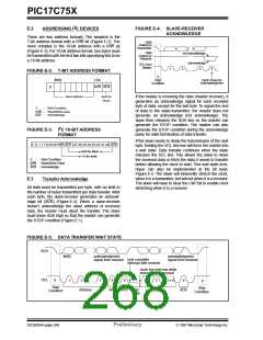
FIGURE E-3: I C 10-BIT ADDRESS
FORMAT
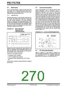
If the slave needs to delay the transmission of the next
byte, holding the SCL line low will force the master into
a wait state. Data transfer continues when the slave
releases the SCL line. This allows the slave to move
the received data or fetch the data it needs to transfer
before allowing the clock to start. This wait state tech-
nique can also be implemented at the bit level,
Figure E-5. The slave will inherently stretch the clock,
when it is a transmitter, but will not when it is a receiver.
The slave will have to clear the CKP bit to enable clock
stretching when it is a receiver.
S
1 1 1 1 0 A9 A8 R/W ACK A7 A6 A5 A4 A3 A2 A1 A0 ACK
sent by slave
= 0 for write
S
- Start Condition
R/W - Read/Write Pulse
ACK - Acknowledge
E.3
Transfer Acknowledge
All data must be transmitted per byte, with no limit to
the number of bytes transmitted per data transfer. After
each byte, the slave-receiver generates an acknowl-
edge bit (ACK) (Figure E-4). When a slave-receiver
doesn’t acknowledge the slave address or received
data, the master must abort the transfer. The slave
must leave SDA high so that the master can generate
the STOP condition (Figure E-1).
FIGURE E-5: DATA TRANSFER WAIT STATE
SDA
MSB
acknowledgment
signal from receiver
acknowledgment
signal from receiver
byte complete
interrupt with receiver
clock line held low while
interrupts are serviced
SCL
S
1
2
7
8
9
1
2
3 • 8
9
P
Start
Condition
Stop
Condition
Address
R/W ACK Wait
State
Data
ACK
DS30264A-page 268
Preliminary
1997 Microchip Technology Inc.

 MICROCHIP [ MICROCHIP ]