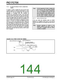
PIC17C75X
2
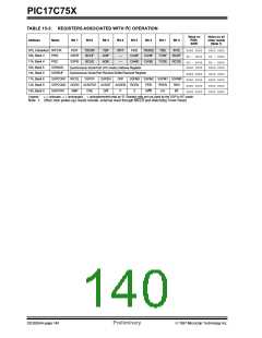
TABLE 15-3: REGISTERS ASSOCIATED WITH I C OPERATION
Value on
POR,
BOR
Value on all
other resets
(Note 1)
Address
Name
Bit 7
Bit 6
Bit 5
Bit 4
Bit 3
Bit 2
Bit 1
Bit 0
07h, Unbanked INTSTA
PEIF
T0CKIF
BCLIF
T0IF
INTF
—
PEIE
T0CKIE
CA3IF
T0IE
INTE
0000 0000
00-- 0000
0000 0000
00-- 0000
10h, Bank 4
11h, Bank 4
PIR2
PIE2
SSPIF
ADIF
CA4IF
TX2IF
RC2IF
SSPIE
BCLIE
ADIE
—
CA4IE
CA3IE
TX2IE
RC2IE
00-- 0000
0000 0000
00-- 0000
0000 0000
Synchronous Serial Port (I2C mode) Address Register
Synchronous Serial Port Receive Buffer/Transmit Register
SSPOV SSPEN CKP SSPM3 SSPM2 SSPM1 SSPM0
GCEN ACKSTAT ACKDT ACKEN
SMP CKE D/A
10h. Bank 6
14h, Bank 6
SSPADD
SSPBUF
xxxx xxxx
0000 0000
0000 0000
0000 0000
uuuu uuuu
0000 0000
0000 0000
0000 0000
11h, Bank 6
12h, Bank 6
13h, Bank 6
Legend:
SSPCON1 WCOL
SSPCON2
SSPSTAT
RCEN
S
PEN
R/W
RSEN
UA
SEN
BF
P
x= unknown, u= unchanged, -= unimplemented read as '0'. Shaded cells are not used by the SSP in I2C mode.
Note 1: Other (non power-up) resets include: external reset through MCLR and Watchdog Timer Reset.
DS30264A-page 140
Preliminary
1997 Microchip Technology Inc.

 MICROCHIP [ MICROCHIP ]