PIC17C75X
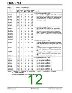
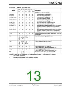
TABLE 3-1:
Name
PINOUT DESCRIPTIONS
DIP PLCC TQFP I/O/P Buffer
Description
No.
No.
No. Type Type
PORTG is a bi-directional I/O Port.
RG0 can also be analog input 3.
RG1 can also be analog input 2.
RG0/AN3
32
31
30
34
33
32
24
23
22
I/O
I/O
I/O
ST
ST
ST
RG1/AN2
RG2/AN1/VREF-
RG2 can also be analog input 1, or
the ground reference voltage
RG3/AN0/VREF+
29
31
21
I/O
ST
RG3 can also be analog input 0, or
the positive reference voltage
RG4/CAP3
35
36
38
38
39
41
27
28
30
I/O
I/O
I/O
ST
ST
ST
RG4 can also be the Capture3 input pin.
RG5 can also be the PWM3 output pin.
RG5/PWM3
RG6/RX2/DT2
RG6 can also be selected as the USART2 (SCI) Asyn-
chronous Receive or USART2 (SCI) Synchronous
Data.
RG7/TX2/CK2
37
40
17
29
8
I/O
ST
ST
RG7 can also be selected as the USART2 (SCI) Asyn-
chronous Transmit or USART2 (SCI) Synchronous
Clock.
TEST
VSS
16
I
Test mode selection control input. Always tie to VSS for nor-
mal operation.
17,
19, 9, 25,
P
Ground reference for logic and I/O pins.
33, 36,53, 41, 56
49,
64
68
VDD
1,
2, 20,
37,
49, 38, 57
10,
26,
P
Positive supply for logic and I/O pins.
18,
34,
46
AVSS
AVDD
NC
28
27
-
30
29
20
19
-
P
P
Ground reference for A/D converter.
This pin MUST be at the same potential as VSS.
Positive supply for A/D converter.
This pin MUST be at the same potential as VDD.
1, 18,
No Connect. Leave these pins unconnected.
35, 52
Legend: I = Input only; O = Output only; I/O = Input/Output; P = Power; — = Not Used; TTL = TTL input;
ST = Schmitt Trigger input.
†
The output is only available by the Peripheral operation.
1997 Microchip Technology Inc.
Preliminary
DS30264A-page 13

 MICROCHIP [ MICROCHIP ]