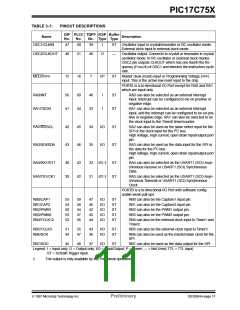
PIC17C75X
TABLE 3-1:
PINOUT DESCRIPTIONS
DIP PLCC TQFP I/O/P Buffer
Name
Description
No.
No.
No. Type Type
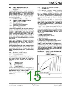
OSC1/CLKIN
47
50
39
I
ST
Oscillator input in crystal/resonator or RC oscillator mode.
External clock input in external clock mode.
OSC2/CLKOUT
MCLR/VPP
48
15
51
16
40
O
—
Oscillator output. Connects to crystal or resonator in crystal
oscillator mode. In RC oscillator or external clock modes
OSC2 pin outputs CLKOUT which has one fourth the fre-
quency (FOSC/4) of OSC1 and denotes the instruction cycle
rate.
7
I/P
ST
Master clear (reset) input or Programming Voltage (VPP)
input. This is the active low reset input to the chip.
PORTA is a bi-directional I/O Port except for RA0 and RA1
which are input only.
RA0/INT
56
41
60
44
48
33
I
I
ST
ST
RA0 can also be selected as an external interrupt
input. Interrupt can be configured to be on positive or
negative edge.
RA1/T0CKI
RA1 can also be selected as an external interrupt
input, and the interrupt can be configured to be on pos-
itive or negative edge. RA1 can also be selected to be
the clock input to the Timer0 timer/counter.
RA2/SS/SCL
RA3/SDI/SDA
42
43
45
46
34
35
I/O
I/O
ST
ST
RA2 can also be used as the slave select input for the
SPI or the clock input for the I C bus.
High voltage, high current, open drain input/output port
pin.
2
RA3 can also be used as the data input for the SPI or
2
the data for the I C bus.
High voltage, high current, open drain input/output port
pin.
RA4/RX1/DT1
RA5/TX1/CK1
40
39
43
42
32
31
I/O †
I/O †
ST
ST
RA4 can also be selected as the USART1 (SCI) Asyn-
chronous Receive or USART1 (SCI) Synchronous
Data.
RA5 can also be selected as the USART1 (SCI) Asyn-
chronous Transmit or USART1 (SCI) Synchronous
Clock.
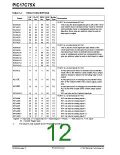
PORTB is a bi-directional I/O Port with software config-
urable weak pull-ups.
RB0/CAP1
RB1/CAP2
RB2/PWM1
RB3/PWM2
RB4/TCLK12
55
54
50
53
52
59
58
54
57
56
47
46
42
45
44
I/O
I/O
I/O
I/O
I/O
ST
ST
ST
ST
ST
RB0 can also be the Capture1 input pin.
RB1 can also be the Capture2 input pin.
RB2 can also be the PWM1 output pin.
RB3 can also be the PWM2 output pin.
RB4 can also be the external clock input to Timer1 and
Timer2.
RB5/TCLK3
RB6/SCK
51
44
55
47
43
36
I/O
I/O
ST
ST
RB5 can also be the external clock input to Timer3.
RB6 can also be used as the master/slave clock for the
SPI.
RB7/SDO
45
48
37
I/O
ST
RB7 can also be used as the data output for the SPI.
Legend: I = Input only; O = Output only; I/O = Input/Output; P = Power; — = Not Used; TTL = TTL input;
ST = Schmitt Trigger input.
†
The output is only available by the Peripheral operation.
1997 Microchip Technology Inc.
Preliminary
DS30264A-page 11

 MICROCHIP [ MICROCHIP ]