PIC17C75X
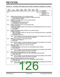
When the application software is expecting to receive
valid data, the SSPBUF should be read before the next
byte of data to transfer is written to the SSPBUF. Buffer
full bit BF (SSPSTAT<0>) indicates when SSPBUF has
been loaded with the received data (transmission is
complete). When the SSPBUF is read, bit BF is
cleared. This data may be irrelevant if the SPI is only a
transmitter. Generally the SSP Interrupt is used to
determine when the transmission/reception has com-
pleted.The SSPBUF must be read and/or written. If the
interrupt method is not going to be used, then software
polling can be done to ensure that a write collision does
not occur. Example 15-1 shows the loading of the
SSPBUF (SSPSR) for data transmission. The shaded
instruction is only required if the received data is mean-
ingful.
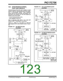
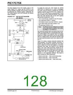
15.1
SPI Mode
The SPI mode allows 8-bits of data to be synchro-
nously transmitted and received simultaneously. All
four modes of SPI are supported. To accomplish com-
munication, typically three pins are used:
• Serial Data Out (SDO)
• Serial Data In (SDI)
• Serial Clock (SCK)
Additionally a fourth pin may be used when in a slave
mode of operation:
• Slave Select (SS)
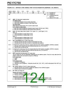
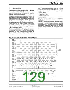
When initializing the SPI, several options need to be
specified.This is done by programming the appropriate
control
bits
in
the
SSPCON1
register
(SSPCON1<5:0>) and SSPSTAT<7:6>. These control
bits allow the following to be specified:
EXAMPLE 15-1: LOADING THE SSPBUF
(SSPSR) REGISTER
• Master Mode (SCK is the clock output)
• Slave Mode (SCK is the clock input)
• Clock Polarity (Idle state of SCK)
• Data input sample phase (middle or end of data
output time)
• Clock edge (output data on rising/falling edge of
SCK)
• Clock Rate (Master mode only)
• Slave Select Mode (Slave mode only)
MOVLB 6
; Bank 6
LOOP BTFSS SSPSTAT, BF
; Has data been
;
received
;
;
(transmit
complete)?
GOTO LOOP
; No
MOVPF SSPBUF, RXDATA ; Save in user RAM
MOVFP TXDATA, SSPBUF ; New data to xmit
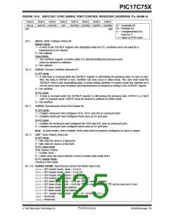
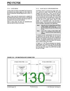
The SSP consists of a transmit/receive Shift Register
(SSPSR) and a buffer register (SSPBUF). The SSPSR
shifts the data in and out of the device, MSb first. The
SSPBUF holds the data that was written to the SSPSR,
until the received data is ready. Once the 8-bits of data
have been received, that byte is moved to the SSPBUF
register. Then the buffer full detect bit BF
(SSPSTAT<0>) and the interrupt flag bit SSPIF
(PIR2<7>) are set. This double buffering of the
received data (SSPBUF) allows the next byte to start
reception before reading the data that was just
received. Any write to the SSPBUF register during
transmission/reception of data will be ignored, and the
write collision detect bit WCOL (SSPCON1<7>) will be
set. User software must clear the WCOL bit so that it
can be determined if the following write(s) to the SSP-
BUF register completed successfully.
1997 Microchip Technology Inc.
Preliminary
DS30264A-page 127

 MICROCHIP [ MICROCHIP ]