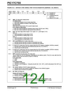
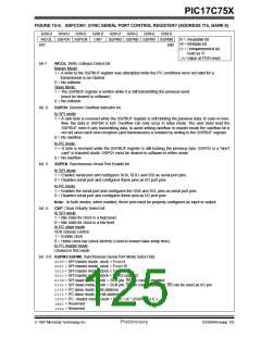
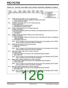
PIC17C75X
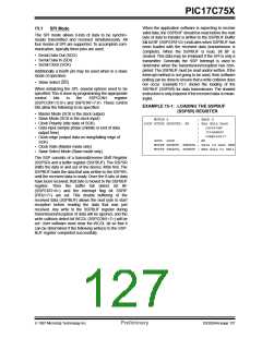
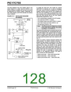
The block diagram of the SSP module, when in SPI
mode (Figure 15-7), shows that the SSPSR is not
directly readable or writable, and can only be accessed
by addressing the SSPBUF register. Additionally, the
SSP status register (SSPSTAT) indicates the various
status conditions.
To enable the serial port, SSP Enable bit, SSPEN
(SSPCON1<5>) must be set. To reset or reconfigure
SPI mode, clear bit SSPEN, re-initialize the SSPCON
registers, and then set bit SSPEN. This configures the
SDI, SDO, SCK, and SS pins as serial port pins. For the
pins to behave as the serial port function, some must
have their data direction bits (in the DDR register)
appropriately programmed. That is:
FIGURE 15-7: SSP BLOCK DIAGRAM
(SPI MODE)
• SDI is automatically controlled by the SPI module
• SDO must have DDRB<7> cleared
Internal
data bus
• SCK (Master mode) must have DDRB<6> cleared
• SCK (Slave mode) must have DDRB<6> set
• SS must have PORTA<2> set
Read
Write
SSPBUF reg
SSPSR reg
Note: The SS pin must be configured as an input
for the slave select to operate.This is done
by writing a ’1’ to PORTA<2>.
Any serial port function that is not desired may be over-
ridden by programming the corresponding data direc-
tion (DDR) register to the opposite value. An example
would be in master mode where you are only sending
data (to a display driver), then both SDI and SS could
be used as general purpose open drain outputs by writ-
ing a ’0’.
shift
clock
SDI
bit0
SDO
Control
Enable
SS
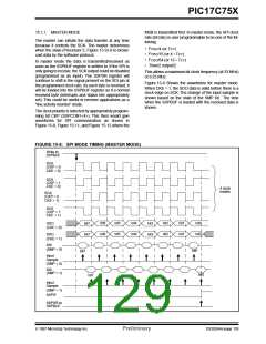
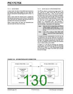
Figure 15-9 shows a typical connection between two
microcontrollers. The master controller (Processor 1)
initiates the data transfer by sending the SCK signal.
Data is shifted out of both shift registers on their pro-
grammed clock edge, and latched on the opposite
edge of the clock. Both processors should be pro-
grammed to same Clock Polarity (CKP), then both con-
trollers would send and receive data at the same time.
Whether the data is meaningful (or dummy data)
depends on the application software. This leads to
three scenarios for data transmission:
SS
Edge
Select
2
Clock Select
SSPM3:SSPM0
SMP:CKE
2
4
TMR2 output
2
Edge
Select
TOSC
Prescaler
4, 16, 64
SCK
• Master sends data — Slave sends dummy data
• Master sends data — Slave sends data
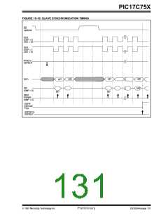
Data to TX/RX in SSPSR
Data direction bit
• Master sends dummy data — Slave sends data
DS30264A-page 128
Preliminary
1997 Microchip Technology Inc.

 MICROCHIP [ MICROCHIP ]