PIC17C75X
15.1.2 SLAVE MODE
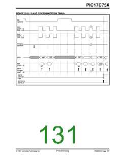
15.1.3 SLAVE SELECT SYNCHRONIZATION
In slave mode, the data is transmitted and received as
the external clock pulses appear on SCK. When the
last bit is latched the interrupt flag bit SSPIF (PIR2<7>)
is set.
The SS pin allows a synchronous slave mode. The
SPI must be in slave mode with SS pin control
enabled (SSPCON1<3:0> = 04h). The pin must not
be driven low for the SS pin to function as an input.
The RA2 Data Latch must be high. When the SS pin
is low, transmission and reception are enabled and
the SDO pin is driven. When the SS pin goes high,
the SDO pin is no longer driven, even if in the
middle of a transmitted byte, and becomes a
floating output. External pull-up/ pull-down resistors
may be desirable, depending on the application.
While in slave mode the external clock is supplied by
the external clock source on the SCK pin.This external
clock must meet the minimum high and low times as
specified in the electrical specifications.
While in sleep mode, the slave can transmit/receive
data and wake the device from sleep.
Note: When the SPI is in Slave Mode with SS pin
control enabled, (SSPCON<3:0> = 0100)
the SPI module will reset if the SS pin is set
to VDD.
Note: If the SPI is used in Slave Mode with
CKE = '1', then the SS pin control must be
enabled.
To emulate two-wire communication, the SDO pin can
be connected to the SDI pin. When the SPI needs to
operate as a receiver the SDO pin can be configured as
an input. This disables transmissions from the SDO.
The SDI can always be left as an input (SDI function)
since it cannot create a bus conflict.
In Figure 15-11 the SS pin terminates the transmis-
sion/reception. The SSPIF bit is set after the last edge
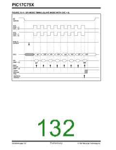
of the SCK. In Figure 15-12 the SS pin causes the first
bit of the data to be output. The SSPIF bit in set after
the last SCK edge.
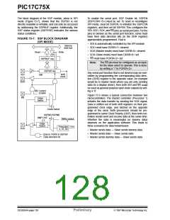
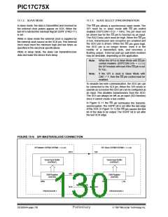
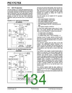
FIGURE 15-9: SPI MASTER/SLAVE CONNECTION
SPI Master SSPM3:SSPM0 = 00xxb
SPI Slave SSPM3:SSPM0 = 010xb
SDO
SDI
Serial Input Buffer
(SSPBUF)
Serial Input Buffer
(SSPBUF)
SDI
SDO
Shift Register
Shift Register
(SSPSR)
(SSPSR)
LSb
MSb
MSb
LSb
Serial Clock
SCK
SCK
PROCESSOR 1
PROCESSOR 2
DS30264A-page 130
Preliminary
1997 Microchip Technology Inc.

 MICROCHIP [ MICROCHIP ]