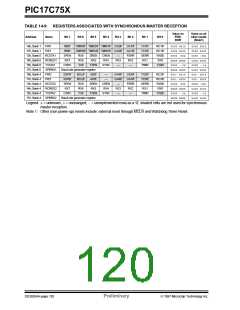
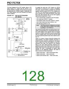
PIC17C75X
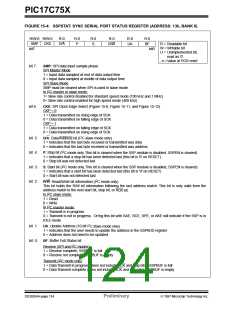
FIGURE 15-4: SSPSTAT: SYNC SERIAL PORT STATUS REGISTER (ADDRESS: 13h, BANK 6)
R/W-0 R/W-0
SMP CKE
bit7
R-0
D/A
R-0
P
R-0
S
R-0
R-0
UA
R-0
BF
R/W
R = Readable bit
W = Writable bit
U = Unimplemented bit,
read as ‘0’
bit0
- n =Value at POR reset
bit 7:
SMP: SPI data input sample phase
SPI Master Mode
1 = Input data sampled at end of data output time
0 = Input data sampled at middle of data output time
SPI Slave Mode
SMP must be cleared when SPI is used in slave mode
2
In I C master or slave mode:
1= Slew rate control disabled for standard speed mode (100 kHz and 1 MHz)
0= Slew rate control enabled for high speed mode (400 kHz)
bit 6:
CKE: SPI Clock Edge Select (Figure 15-8, Figure 15-11, and Figure 15-12)
CKP = 0
1 = Data transmitted on rising edge of SCK
0 = Data transmitted on falling edge of SCK
CKP = 1
1 = Data transmitted on falling edge of SCK
0 = Data transmitted on rising edge of SCK
2
bit 5:
bit 4:
bit 3:
bit 2:
D/A: Data/Address bit (I C slave mode only)
1 = Indicates that the last byte received or transmitted was data
0 = Indicates that the last byte received or transmitted was address
2
P: Stop bit (I C mode only. This bit is cleared when the SSP module is disabled, SSPEN is cleared)
1 = Indicates that a stop bit has been detected last (this bit is '0' on RESET)
0 = Stop bit was not detected last
2
S: Start bit (I C mode only. This bit is cleared when the SSP module is disabled, SSPEN is cleared)
1 = Indicates that a start bit has been detected last (this bit is '0' on RESET)
0 = Start bit was not detected last
2
R/W: Read/Write bit information (I C mode only)
This bit holds the R/W bit information following the last address match. This bit is only valid from the
address match to the next start bit, stop bit, or ACK bit.
2
In I C slave mode:
1 = Read
0 = Write
2
In I C master mode:
1 = Transmit is in progress
0 = Transmit is not in progress. Or’ing this bit with SAE, RCE, SPE, or AKE will indicate if the SSP is in
IDLE mode.
2
bit 1:
bit 0:
UA: Update Address (10-bit I C slave mode only)
1 = Indicates that the user needs to update the address in the SSPADD register
0 = Address does not need to be updated
BF: Buffer Full Status bit
2
Receive (SPI and I C modes)
1 = Receive complete, SSPBUF is full
0 = Receive not complete, SSPBUF is empty
2
Transmit (I C mode only)
1 = Data Transmit in progress (does not include ACK and stop bits), SSPBUF is full
0 = Data Transmit complete (does not include ACK and stop bits), SSPBUF is empty
DS30264A-page 124
Preliminary
1997 Microchip Technology Inc.

 MICROCHIP [ MICROCHIP ]