PIC17C75X
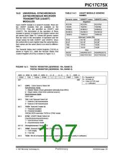
TABLE 14-1: USART MODULE GENERIC
NAMES
14.0 UNIVERSAL SYNCHRONOUS
ASYNCHRONOUS RECEIVER
TRANSMITTER (USART)
MODULES
Generic name
USART1 name USART2 name
Registers
RCSTA
TXSTA
SPBRG
RCREG
TXREG
RCSTA1
TXSTA1
RCSTA2
TXSTA2
SPBRG2
RCREG2
TXREG2
Each USART module is a serial I/O module. There are
two USART modules that are available on the
PIC17C75X. They are specified as USART1 and
USART2. The description of the operation of these
modules is generic in regard to the register names and
pin names used. Table 14-1 shows the generic names
that are used in the description of operation and the
actual names for both USART1 and USART2. Since
the control bits in each register have the same function,
their names are the same (there is no need to differen-
tiate).
SPBRG1
RCREG1
TXREG1
Interrupt Control Bits
RC1IE
RCIE
RCIF
TXIE
TXIF
RC2IE
RC2IF
TX2IE
TX2IF
RC1IF
TX1IE
TX1IF
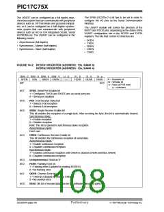
The Transmit Status And Control Register (TXSTA) is
shown in Figure 14-1, while the Receive Status And
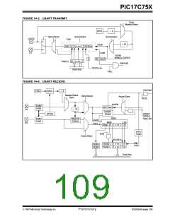
Control Register (RCSTA) is shown in Figure 14-2.
Pins
RX/DT
TX/CK
RA4/RX1/DT1
RA5/TX1/CK1
RG6/RX2/DT2
RG7/TX2/CK2
FIGURE 14-1: TXSTA1 REGISTER (ADDRESS: 15h, BANK 0)
TXSTA2 REGISTER (ADDRESS: 15h, BANK 4)
R/W - 0 R/W - 0 R/W - 0 R/W - 0
CSRC TX9 TXEN SYNC
bit7
U - 0
—
U - 0
—
R - 1
TRMT
R/W - x
TX9D
bit0
R = Readable bit
W = Writable bit
-n = Value at POR reset
(x = unknown)
bit 7:
CSRC: Clock Source Select bit
Synchronous mode:
1 = Master Mode (Clock generated internally from BRG)
0 = Slave mode (Clock from external source)
Asynchronous mode:
Don’t care
bit 6:
bit 5:
TX9: 9-bit Transmit Select bit
1 = Selects 9-bit transmission
0 = Selects 8-bit transmission
TXEN: Transmit Enable bit
1 = Transmit enabled
0 = Transmit disabled
SREN/CREN overrides TXEN in SYNC mode
bit 4:
SYNC: USART Mode Select bit
(Synchronous/Asynchronous)
1 = Synchronous mode
0 = Asynchronous mode
bit 3-2: Unimplemented: Read as '0'
bit 1:
TRMT: Transmit Shift Register (TSR) Empty bit
1 = TSR empty
0 = TSR full
bit 0:
TX9D: 9th bit of transmit data (can be used to calculated the parity in software)
1997 Microchip Technology Inc.
Preliminary
DS30264A-page 107

 MICROCHIP [ MICROCHIP ]