PIC16F913/914/916/917/946
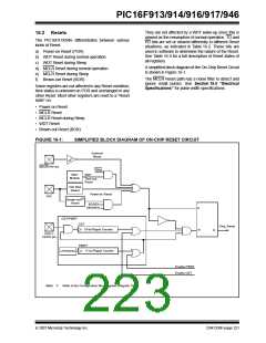
16.1 Configuration Bits
Note:
Address 2007h is beyond the user
program memory space. It belongs to the
special configuration memory space
(2000h-3FFFh), which can be accessed
The Configuration bits can be programmed (read as
‘0’), or left unprogrammed (read as ‘1’) to select various
device configurations as shown in Register 16-1.
These bits are mapped in program memory location
2007h.
only
during
programming.
See
“PIC16F91X/946 Memory Programming
Specification”
(DS41244)
for
more
information.
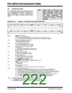
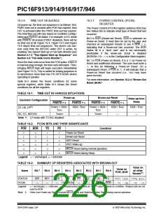
REGISTER 16-1: CONFIG1: CONFIGURATION WORD REGISTER 1
—
—
—
DEBUG
FCMEN
IESO
BOREN1
FOSC1
BOREN0
bit 15
bit 8
CPD
CP
MCLRE
PWRTE
WDTE
FOSC2
FOSC0
bit 7
bit 0
bit 15-13
bit 12
Unimplemented: Read as ‘1’
DEBUG: In-Circuit Debugger Mode bit
1= In-Circuit Debugger disabled, RB6/ICSPCLK and RB7/ICSPDAT are general purpose I/O pins
0= In-Circuit Debugger enabled, RB6/ICSPCLK and RB7/ICSPDAT are dedicated to the debugger
bit 11
bit 10
bit 9-8
FCMEN: Fail-Safe Clock Monitor Enabled bit
1= Fail-Safe Clock Monitor is enabled
0= Fail-Safe Clock Monitor is disabled
IESO: Internal External Switchover bit
1= Internal/External Switchover mode is enabled
0= Internal/External Switchover mode is disabled
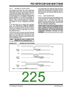
BOREN<1:0>: Brown-out Reset Selection bits(1)
11= BOR enabled
10= BOR enabled during operation and disabled in Sleep
01= BOR controlled by SBOREN bit of the PCON register
00= BOR disabled
bit 7
bit 6
bit 5
bit 4
bit 3
bit 2-0
CPD: Data Code Protection bit(2)
1= Data memory code protection is disabled
0= Data memory code protection is enabled
CP: Code Protection bit(3)
1= Program memory code protection is disabled
0= Program memory code protection is enabled
MCLRE: RE3/MCLR pin function select bit(4)
1= RE3/MCLR pin function is MCLR
0= RE3/MCLR pin function is digital input, MCLR internally tied to VDD
PWRTE: Power-up Timer Enable bit
1= PWRT disabled
0= PWRT enabled
WDTE: Watchdog Timer Enable bit
1= WDT enabled
0= WDT disabled and can be enabled by SWDTEN bit of the WDTCON register
FOSC<2:0>: Oscillator Selection bits
111= RC oscillator: CLKOUT function on RA6/OSC2/CLKOUT/T1OSO pin, RC on RA7/OSC1/CLKIN/T1OSI
110= RCIO oscillator: I/O function on RA6/OSC2/CLKOUT/T1OSO pin, RC on RA7/OSC1/CLKIN/T1OSI
101= INTOSC oscillator: CLKOUT function on RA6/OSC2/CLKOUT/T1OSO pin, I/O function on RA7/OSC1/CLKIN/T1OSI
100= INTOSCIO oscillator: I/O function on RA6/OSC2/CLKOUT/T1OSO pin, I/O function on RA7/OSC1/CLKIN/T1OSI
011= EC: I/O function on RA6/OSC2/CLKOUT/T1OSO pin, CLKIN on RA7/OSC1/CLKIN/T1OSI
010= HS oscillator: High-speed crystal/resonator on RA6/OSC2/CLKOUT/T1OSO and RA7/OSC1/CLKIN/T1OSI
001= XT oscillator: Crystal/resonator on RA6/OSC2/CLKOUT/T1OSO and RA7/OSC1/CLKIN/T1OSI
000= LP oscillator: Low-power crystal on RA6/OSC2/CLKOUT/T1OSO and RA7/OSC1/CLKIN/T1OSI
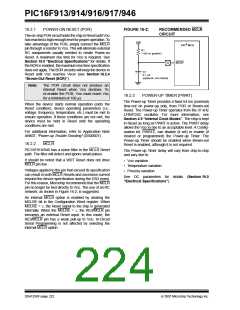
Note 1:
Enabling Brown-out Reset does not automatically enable Power-up Timer.
The entire data EEPROM will be erased when the code protection is turned off.
The entire program memory will be erased when the code protection is turned off.
When MCLR is asserted in INTOSC or RC mode, the internal clock oscillator is disabled.
2:
3:
4:
DS41250F-page 220
© 2007 Microchip Technology Inc.

 MICROCHIP [ MICROCHIP ]