PIC16F913/914/916/917/946
16.2.1
POWER-ON RESET (POR)
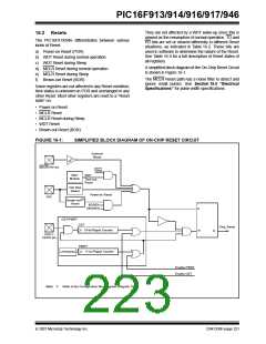
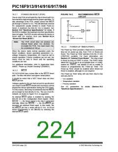
FIGURE 16-2:
RECOMMENDED MCLR
CIRCUIT
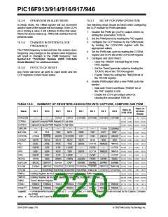
The on-chip POR circuit holds the chip in Reset until VDD
has reached a high enough level for proper operation. To
take advantage of the POR, simply connect the MCLR
pin through a resistor to VDD. This will eliminate external
RC components usually needed to create Power-on
Reset. A maximum rise time for VDD is required. See
Section 19.0 “Electrical Specifications” for details. If
the BOR is enabled, the maximum rise time specification
does not apply. The BOR circuitry will keep the device in
Reset until VDD reaches VBOR (see Section 16.2.4
“Brown-Out Reset (BOR)”).
VDD
R1
PIC® MCU
1 kΩ (or greater)
MCLR
C1
0.1 μF
(optional, not critical)
Note:
The POR circuit does not produce an
internal Reset when VDD declines. To
re-enable the POR, VDD must reach Vss
for a minimum of 100 μs.
16.2.3
POWER-UP TIMER (PWRT)
The Power-up Timer provides a fixed 64 ms (nominal)
time-out on power-up only, from POR or Brown-out
Reset. The Power-up Timer operates from the 31 kHz
LFINTOSC oscillator. For more information, see
Section 4.5 “Internal Clock Modes”. The chip is kept
in Reset as long as PWRT is active. The PWRT delay
allows the VDD to rise to an acceptable level. A Config-
uration bit, PWRTE, can disable (if set) or enable (if
cleared or programmed) the Power-up Timer. The
Power-up Timer should be enabled when Brown-out
Reset is enabled, although it is not required.
When the device starts normal operation (exits the
Reset condition), device operating parameters (i.e.,
voltage, frequency, temperature, etc.) must be met to
ensure operation. If these conditions are not met, the
device must be held in Reset until the operating
conditions are met.
For additional information, refer to Application Note
AN607, “Power-up Trouble Shooting” (DS00607).
16.2.2
MCLR
PIC16F91X/946 has a noise filter in the MCLR Reset
path. The filter will detect and ignore small pulses.
The Power-up Timer delay will vary from chip-to-chip
and vary due to:
It should be noted that a WDT Reset does not drive
MCLR pin low.
• VDD variation
• Temperature variation
• Process variation
Voltages applied to the pin that exceed its specification
can result in both MCLR Resets and excessive current
beyond the device specification during the ESD event.
For this reason, Microchip recommends that the MCLR
pin no longer be tied directly to VDD. The use of an RC
network, as shown in Figure 16-2, is suggested.
See DC parameters for details (Section 19.0
“Electrical Specifications”).
An internal MCLR option is enabled by clearing the
MCLRE bit in the Configuration Word register. When
MCLRE = 0, the Reset signal to the chip is generated
internally. When the MCLRE = 1, the RE3/MCLR pin
becomes an external Reset input. In this mode, the
RE3/MCLR pin has a weak pull-up to VDD. In-Circuit
Serial Programming is not affected by selecting the
internal MCLR option.
DS41250F-page 222
© 2007 Microchip Technology Inc.

 MICROCHIP [ MICROCHIP ]