PIC16F913/914/916/917/946
16.2.6
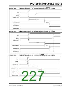
TIME-OUT SEQUENCE
16.2.7
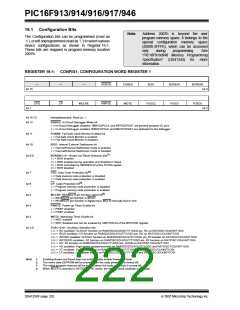
POWER CONTROL (PCON)
REGISTER
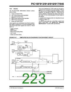
On power-up, the time-out sequence is as follows: first,
PWRT time-out is invoked after POR has expired, then
OST is activated after the PWRT time-out has expired.
The total time-out will vary based on oscillator configu-
ration and PWRTE bit status. For example, in EC mode
with PWRTE bit erased (PWRT disabled), there will be
no time-out at all. Figure 16-4, Figure 16-5 and Figure
16-6 depict time-out sequences. The device can exe-
cute code from the INTOSC while OST is active, by
enabling Two-Speed Start-up or Fail-Safe Monitor (see
Section 4.7.2 “Two-Speed Start-up Sequence” and
Section 4.8 “Fail-Safe Clock Monitor”).
The Power Control (PCON) register (address 8Eh) has
two Status bits to indicate what type of Reset that last
occurred.
Bit 0 is BOR (Brown-out Reset). BOR is unknown on
Power-on Reset. It must then be set by the user and
checked on subsequent Resets to see if BOR = 0,
indicating that a Brown-out has occurred. The BOR
Status bit is a “don’t care” and is not necessarily
predictable if the brown-out circuit is disabled
(BOREN<1:0> = 00in the Configuration Word register).
Bit 1 is POR (Power-on Reset). It is a ‘0’ on Power-on
Reset and unaffected otherwise. The user must write a
‘1’ to this bit following a Power-on Reset. On a
subsequent Reset, if POR is ‘0’, it will indicate that a
Power-on Reset has occurred (i.e., VDD may have
gone too low).
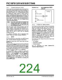
Since the time-outs occur from the POR pulse, if MCLR
is kept low long enough, the time-outs will expire. Then,
bringing MCLR high will begin execution immediately
(see Figure 16-5). This is useful for testing purposes or
to synchronize more than one PIC16F91X/946 device
operating in parallel.
For more information, see Section 16.2.4 “Brown-Out
Reset (BOR)”.
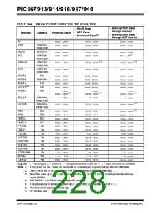
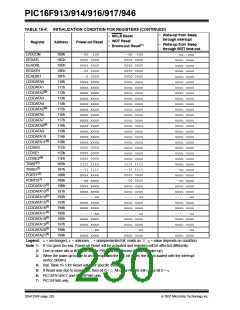
Table 16-5 shows the Reset conditions for some
special registers, while Table 16-5 shows the Reset
conditions for all the registers.
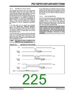
TABLE 16-1: TIME-OUT IN VARIOUS SITUATIONS
Power-up
Brown-out Reset
Wake-up from
Oscillator Configuration
Sleep
PWRTE = 0
PWRTE = 1
PWRTE = 0
PWRTE = 1
XT, HS, LP(1)
TPWRT + 1024 •
TOSC
1024 • TOSC
TPWRT + 1024 •
TOSC
1024 • TOSC
1024 • TOSC
—
RC, EC, INTOSC
TPWRT
—
TPWRT
—
Note 1: LP mode with T1OSC disabled.
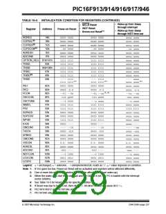
TABLE 16-2: PCON BITS AND THEIR SIGNIFICANCE
POR
BOR
TO
PD
Condition
0
1
u
u
u
0
u
u
1
1
0
0
1
1
u
0
Power-on Reset
Brown-out Reset
WDT Reset
WDT Wake-up
u
u
u
u
u
1
u
0
MCLR Reset during normal operation
MCLR Reset during Sleep
Legend: u= unchanged, x= unknown
TABLE 16-3: SUMMARY OF REGISTERS ASSOCIATED WITH BROWN-OUT
Value on
all other
Resets(1)
Value on
POR, BOR
Name
Bit 7
Bit 6
Bit 5
Bit 4
Bit 3
Bit 2
Bit 1
Bit 0
STATUS
IRP
—
RP1
—
RP0
—
TO
PD
—
Z
DC
C
0001 1xxx 000q quuu
--01 --qq --0u --uu
PCON
SBOREN
—
POR
BOR
Legend:
u= unchanged, x= unknown, -= unimplemented bit, reads as ‘0’, q= value depends on condition. Shaded cells are not
used by BOR.
Note 1: Other (non Power-up) Resets include MCLR Reset and Watchdog Timer Reset during normal operation.
DS41250F-page 224
© 2007 Microchip Technology Inc.

 MICROCHIP [ MICROCHIP ]