PIC16F913/914/916/917/946
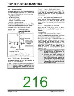
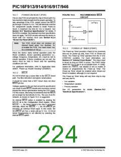
15.3.4
OPERATION IN SLEEP MODE
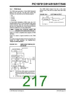
15.3.7
SETUP FOR PWM OPERATION
In Sleep mode, the TMR2 register will not increment
and the state of the module will not change. If the CCPx
pin is driving a value, it will continue to drive that value.
When the device wakes up, TMR2 will continue from its
previous state.
The following steps should be taken when configuring
the CCP module for PWM operation:
1. Disable the PWM pin (CCPx) output drivers by
setting the associated TRIS bit.
2. Set the PWM period by loading the PR2 register.
3. Configure the CCP module for the PWM mode
by loading the CCPxCON register with the
appropriate values.
15.3.5
CHANGES IN SYSTEM CLOCK
FREQUENCY
The PWM frequency is derived from the system clock
frequency. Any changes in the system clock frequency
will result in changes to the PWM frequency. See
Section 4.0 “Oscillator Module (With Fail-Safe
Clock Monitor)” for additional details.
4. Set the PWM duty cycle by loading the CCPRxL
register and CCPx bits of the CCPxCON register.
5. Configure and start Timer2:
• Clear the TMR2IF interrupt flag bit of the
PIR1 register.
15.3.6
EFFECTS OF RESET
• Set the Timer2 prescale value by loading the
T2CKPS bits of the T2CON register.
Any Reset will force all ports to Input mode and the
CCP registers to their Reset states.
• Enable Timer2 by setting the TMR2ON bit of
the T2CON register.
6. Enable PWM output after a new PWM cycle has
started:
• Wait until Timer2 overflows (TMR2IF bit of
the PIR1 register is set).
• Enable the CCPx pin output driver by
clearing the associated TRIS bit.
TABLE 15-5: SUMMARY OF REGISTERS ASSOCIATED WITH CAPTURE, COMPARE AND PWM
Value on
Value on
POR, BOR
Name
Bit 7
Bit 6
Bit 5
Bit 4
Bit 3
Bit 2
Bit 1
Bit 0
all other
Resets
CCPxCON
CCPRxL
CCPRxH
CMCON1
INTCON
—
—
CCPxX
CCPxY
CCPxM3 CCPxM2 CCPxM1 CCPxM0 --00 0000 --00 0000
xxxx xxxx uuuu uuuu
Capture/Compare/PWM Register X Low Byte
Capture/Compare/PWM Register X High Byte
xxxx xxxx uuuu uuuu
—
—
—
—
INTE
—
RBIE
CS1
—
---- --10
C2SYNC ---- --10
T1GSS
INTF
GIE
PEIE
SLPEN
SE14
ADIE
C2IE
T0IE
T0IF
RBIF
0000 000x 0000 000x
LCDCON
LCDSE1
PIE1
LCDEN
SE15
EEIE
WERR
SE13
RCIE
C1IE
VLCDEN
SE12
TXIE
CS0
LMUX1
SE9
LMUX0 0001 0011 0001 0011
SE8 0000 0000 0000 0000
SE11
SSPIE
—
SE10
CCP1IE
LVDIE
CCP1IF
LVDIF
FERR
SSPM2
TMR2IE
—
TMR1IE 0000 0000 0000 0000
CCP2IE 0000 -0-0 0000 -0-0
TMR1IF 0000 0000 0000 0000
CCP2IF 0000 -0-0 0000 -0-0
PIE2
OSFIE
EEIF
LCDIE
TXIF
PIR1
ADIF
C2IF
RCIF
C1IF
SSPIF
—
TMR2IF
—
PIR2
OSFIF
SPEN
WCOL
LCDIF
CREN
CKP
RCSTA
SSPCON
T1CON
T2CON
TMR1L
TMR1H
TMR2
RX9
SREN
SSPEN
ADDEN
SSPM3
OERR
SSPM1
RX9D
0000 000x 0000 000x
SSPOV
SSPM0 0000 0000 0000 0000
T1GINV TMR1GE T1CKPS1 T1CKPS0 T1OSCEN T1SYNC TMR1CS TMR1ON 0000 0000 uuuu uuuu
-000 0000 -000 0000
xxxx xxxx uuuu uuuu
—
TOUTPS3 TOUTPS2 TOUTPS1 TOUTPS0 TMR2ON T2CKPS1 T2CKPS0
Holding Register for the Least Significant Byte of the 16-bit TMR1 Register
Holding Register for the Most Significant Byte of the 16-bit TMR1 Register
Timer2 Module Register
xxxx xxxx uuuu uuuu
0000 0000 0000 0000
TRISC
TRISD(1)
TRISC7
TRISD7
TRISC6
TRISD6
TRISC5
TRISD5
TRISC4
TRISD4
TRISC3
TRISD3
TRISC2
TRISD2
TRISC1
TRISD1
TRISC0 1111 1111 1111 1111
1111 1111
TRISD0 1111 1111
Legend: -= Unimplemented locations, read as ‘0’, u= unchanged, x= unknown. Shaded cells are not used by the Capture, Compare
and PWM.
Note 1: PIC16F914/917 and PIC16F946 only.
DS41250F-page 218
© 2007 Microchip Technology Inc.

 MICROCHIP [ MICROCHIP ]