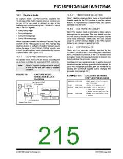
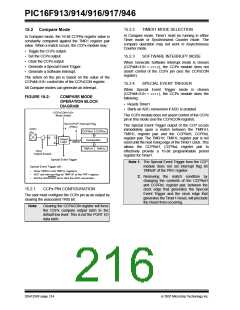
PIC16F913/914/916/917/946
15.3.1
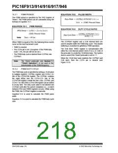
PWM PERIOD
EQUATION 15-2: PULSE WIDTH
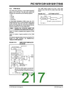
The PWM period is specified by the PR2 register of
Timer2. The PWM period can be calculated using the
formula of Equation 15-1.
Pulse Width = (CCPRxL:CCPxCON<5:4>) •
TOSC • (TMR2 Prescale Value)
EQUATION 15-1: PWM PERIOD
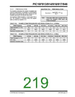
EQUATION 15-3: DUTY CYCLE RATIO
PWM Period = [(PR2) + 1] • 4 • TOSC •
(TMR2 Prescale Value)
(CCPRxL:CCPxCON<5:4>)
Duty Cycle Ratio = ----------------------------------------------------------------------
4(PR2 + 1)
Note:
TOSC = 1/FOSC
The CCPRxH register and a 2-bit internal latch are
used to double buffer the PWM duty cycle. This double
buffering is essential for glitchless PWM operation.
When TMR2 is equal to PR2, the following three events
occur on the next increment cycle:
• TMR2 is cleared
The 8-bit timer TMR2 register is concatenated with
either the 2-bit internal system clock (FOSC), or 2 bits of
the prescaler, to create the 10-bit time base. The system
clock is used if the Timer2 prescaler is set to 1:1.
• The CCPx pin is set. (Exception: If the PWM duty
cycle = 0%, the pin will not be set.)
• The PWM duty cycle is latched from CCPRxL into
CCPRxH.
When the 10-bit time base matches the CCPRxH and
2-bit latch, then the CCPx pin is cleared (see
Figure 15-3).
Note:
The Timer2 postscaler (see Section 7.1
“Timer2 Operation”) is not used in the
determination of the PWM frequency.
15.3.2
PWM DUTY CYCLE
The PWM duty cycle is specified by writing a 10-bit value
to multiple registers: CCPRxL register and CCPx<1:0>
bits of the CCPxCON register. The CCPRxL contains
the eight MSbs and the CCPx<1:0> bits of the
CCPxCON register contain the two LSbs. CCPRxL and
CCPx<1:0> bits of the CCPxCON register can be written
to at any time. The duty cycle value is not latched into
CCPRxH until after the period completes (i.e., a match
between PR2 and TMR2 registers occurs). While using
the PWM, the CCPRxH register is read-only.
Equation 15-2 is used to calculate the PWM pulse
width.
Equation 15-3 is used to calculate the PWM duty cycle
ratio.
DS41250F-page 216
© 2007 Microchip Technology Inc.

 MICROCHIP [ MICROCHIP ]