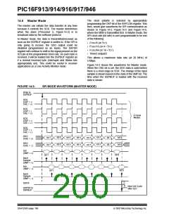
PIC16F913/914/916/917/946
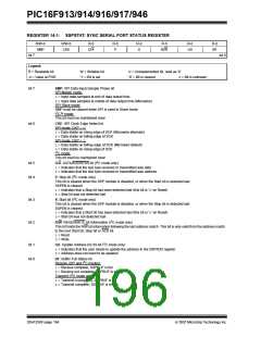
REGISTER 14-1: SSPSTAT: SYNC SERIAL PORT STATUS REGISTER
R/W-0
SMP
R/W-0
CKE
R-0
D/A
R-0
P
R-0
S
R-0
R-0
UA
R-0
BF
R/W
bit 7
bit 0
Legend:
R = Readable bit
-n = Value at POR
W = Writable bit
‘1’ = Bit is set
U = Unimplemented bit, read as ‘0’
‘0’ = Bit is cleared x = Bit is unknown
bit 7
SMP: SPI Data Input Sample Phase bit
SPI Master mode:
1= Input data sampled at end of data output time
0= Input data sampled at middle of data output time (Microwire)
SPI Slave mode:
SMP must be cleared when SPI is used in Slave mode
2
I C™ mode:
This bit must be maintained clear
bit 6
CKE: SPI Clock Edge Select bit
SPI mode, CKP = 0:
1= Data stable on rising edge of SCK (Microwire alternate)
0= Data stable on falling edge of SCK
SPI mode, CKP = 1:
1= Data stable on falling edge of SCK (Microwire default)
0= Data stable on rising edge of SCK
2
I C mode:
This bit must be maintained clear
2
bit 5
bit 4
D/A: DATA/ADDRESS bit (I C mode only)
1= Indicates that the last byte received or transmitted was data
0= Indicates that the last byte received or transmitted was address
2
P: Stop bit (I C mode only)
This bit is cleared when the SSP module is disabled, or when the Start bit is detected last.
SSPEN is cleared.
1= Indicates that a Stop bit has been detected last (this bit is ‘0’ on Reset)
0= Stop bit was not detected last
2
bit 3
bit 2
S: Start bit (I C mode only)
This bit is cleared when the SSP module is disabled, or when the Stop bit is detected last.
SSPEN is cleared.
1= Indicates that a Start bit has been detected last (this bit is ‘0’ on Reset)
0= Start bit was not detected last
2
R/W: READ/WRITE bit Information (I C mode only)
This bit holds the R/W bit information following the last address match. This bit is only valid from the address match
to the next Start bit, Stop bit or ACK bit.
1= Read
0= Write
2
bit 1
bit 0
UA: Update Address bit (10-bit I C mode only)
1= Indicates that the user needs to update the address in the SSPADD register
0= Address does not need to be updated
BF: Buffer Full Status bit
2
Receive (SPI and I C modes):
1= Receive complete, SSPBUF is full
0= Receive not complete, SSPBUF is empty
2
Transmit (I C mode only):
1= Transmit in progress, SSPBUF is full
0= Transmit complete, SSPBUF is empty
DS41250F-page 194
© 2007 Microchip Technology Inc.

 MICROCHIP [ MICROCHIP ]