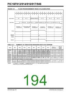
PIC16F913/914/916/917/946
When the application software is expecting to receive
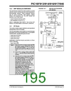
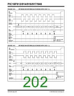
14.2 Operation
valid data, the SSPBUF should be read before the next
byte of data to transfer is written to the SSPBUF. Buffer
Full bit BF of the SSPSTAT register indicates when
SSPBUF has been loaded with the received data
(transmission is complete). When the SSPBUF is read,
the BF bit is cleared. This data may be irrelevant if the
SPI is only a transmitter. Generally, the SSP interrupt is
used to determine when the transmission/reception
has completed. The SSPBUF must be read and/or
written. If the interrupt method is not going to be used,
then software polling can be done to ensure that a write
collision does not occur. Example 14-1 shows the
loading of the SSPBUF (SSPSR) for data transmission.
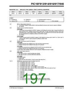
When initializing the SPI, several options need to be
specified. This is done by programming the appropriate
control bits (SSPCON<5:0> and SSPSTAT<7:6>).
These control bits allow the following to be specified:
• Master mode (SCK is the clock output)
• Slave mode (SCK is the clock input)
• Clock Polarity (Idle state of SCK)
• Data Input Sample Phase (middle or end of data
output time)
• Clock Edge (output data on rising/falling edge of
SCK)
• Clock Rate (Master mode only)
The SSPSR is not directly readable or writable and can
only be accessed by addressing the SSPBUF register.
Additionally, the SSP STATUS register (SSPSTAT)
indicates the various status conditions.
• Slave Select mode (Slave mode only)
The SSP consists of a transmit/receive shift register
(SSPSR) and a buffer register (SSPBUF). The SSPSR
shifts the data in and out of the device, MSb first. The
SSPBUF holds the data that was written to the SSPSR
until the received data is ready. Once the eight bits of
data have been received, that byte is moved to the
SSPBUF register. Then, the Buffer Full Status bit BF of
the SSPSTAT register, and the interrupt flag bit SSPIF,
are set. Any write to the SSPBUF register during
transmission/reception of data will be ignored and the
Write Collision Detect bit, WCOL of the SSPCON
register, will be set. User software must clear the
WCOL bit so that it can be determined if the following
write(s) to the SSPBUF register completed
successfully.
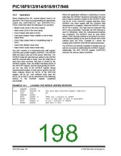
EXAMPLE 14-1:
LOADING THE SSPBUF (SSPSR) REGISTER
BANKSEL
BTFSS
GOTO
SSPSTAT
SSPSTAT, BF
LOOP
;
LOOP
;Has data been received(transmit complete)?
;No
BANKSEL
MOVF
MOVWF
MOVF
SSPBUF
SSPBUF, W
RXDATA
TXDATA, W
SSPBUF
;
;WREG reg = contents of SSPBUF
;Save in user RAM, if data is meaningful
;W reg = contents of TXDATA
;New data to xmit
MOVWF
DS41250F-page 196
© 2007 Microchip Technology Inc.

 MICROCHIP [ MICROCHIP ]