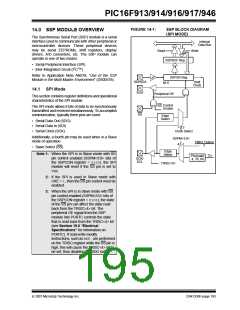
PIC16F913/914/916/917/946
14.3 Enabling SPI I/O
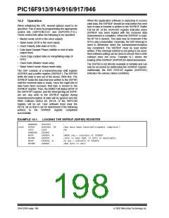
14.4 Typical Connection
To enable the serial port, SSP Enable bit SSPEN of the
SSPCON register must be set. To reset or reconfigure
SPI mode, clear the SSPEN bit, re-initialize the
SSPCON registers and then set the SSPEN bit. This
configures the SDI, SDO, SCK and SS pins as serial
port pins. For the pins to behave as the serial port
function, their data direction bits (in the TRISA and
TRISC registers) should be set as follows:
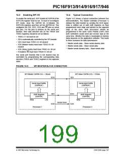
Figure 14-2 shows a typical connection between two
microcontrollers. The master controller (Processor 1)
initiates the data transfer by sending the SCK signal.
Data is shifted out of both shift registers on their
programmed clock edge and latched on the opposite
edge of the clock. Both processors should be
programmed to the same Clock Polarity (CKP), then
both controllers would send and receive data at the
same time. Whether the data is meaningful (or dummy
data) depends on the application software. This leads
to three scenarios for data transmission:
• TRISC<7> bit must be set
• SDI is automatically controlled by the SPI module
• SDO must have TRISC<4> bit cleared
• Master sends data – Slave sends dummy data
• Master sends data – Slave sends data
• SCK (Master mode) must have TRISC<6> bit
cleared
• Master sends dummy data – Slave sends data
• SCK (Slave mode) must have TRISC<6> bit set
• If enabled, SS must have TRISA<5> bit set
Any serial port function that is not desired may be
overridden by programming the corresponding data
direction (TRISA and TRISC) registers to the opposite
value.
FIGURE 14-2:
SPI MASTER/SLAVE CONNECTION
SPI Master SSPM<3:0> = 00xxb
SPI Slave SSPM<3:0> = 010xb
SDI
SDO
Serial Input Buffer
(SSPBUF)
Serial Input Buffer
(SSPBUF)
SDI
SDO
Shift Register
(SSPSR)
Shift Register
(SSPSR)
LSb
MSb
MSb
LSb
Serial Clock
SCK
SCK
Processor 1
Processor 2
© 2007 Microchip Technology Inc.
DS41250F-page 197

 MICROCHIP [ MICROCHIP ]