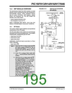
PIC16F913/914/916/917/946
The steps to write to EEPROM data memory are:
13.1.2
READING THE DATA EEPROM
MEMORY
1. If step 10 is not implemented, check the WR bit
to see if a write is in progress.
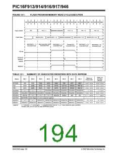
To read a data memory location, the user must write the
address to the EEADRL register, clear the EEPGD
control bit, and then set control bit RD of the EECON1
register. The data is available in the very next cycle, in
the EEDATL register; therefore, it can be read in the
next instruction. EEDATL will hold this value until
another read or until it is written to by the user (during
a write operation).
2. Write the address to EEADRL. Make sure that
the address is not larger than the memory size
of the device.
3. Write the 8-bit data value to be programmed in
the EEDATL register.
4. Clear the EEPGD bit to point to EEPROM data
memory.
5. Set the WREN bit to enable program operations.
6. Disable interrupts (if enabled).
EXAMPLE 13-1:
DATA EEPROM READ
BANKSELEEADRL
;
7. Execute the special five instruction sequence:
MOVF
MOVWF
DATA_EE_ADDR,W ;Data Memory
EEADRL ;Address to read
• Write 55h to EECON2 in two steps (first to W,
then to EECON2)
BANKSELEECON1
;
BCF
EECON1,EEPGD
;Point to Data
;memory
;EE Read
• Write AAh to EECON2 in two steps (first to
W, then to EECON2)
BSF
EECON1,RD
• Set the WR bit
BANKSELEEDATL
MOVF EEDATL,W
;
8. Enable interrupts (if using interrupts).
;W = EEPROM Data
9. Clear the WREN bit to disable program
operations.
13.1.3
WRITING TO THE DATA EEPROM
MEMORY
10. At the completion of the write cycle, the WR bit
is cleared and the EEIF interrupt flag bit is set.
(EEIF must be cleared by firmware.) If step 1 is
not implemented, then firmware should check
for EEIF to be set, or WR to clear, to indicate the
end of the program cycle.
To write an EEPROM data location, the user must first
write the address to the EEADRL register and the data
to the EEDATL register. Then the user must follow a
specific sequence to initiate the write for each byte.
The write will not initiate if the sequence described below
is not followed exactly (write 55h to EECON2, write AAh
to EECON2, then set WR bit) for each byte. Interrupts
should be disabled during this code segment.
EXAMPLE 13-2:
DATA EEPROM WRITE
BANKSELEECON1
;
BTFSC
GOTO
EECON1,WR
$-1
;Wait for write
;to complete
;
Additionally, the WREN bit in EECON1 must be set to
enable write. This mechanism prevents accidental
writes to data EEPROM due to errant (unexpected)
code execution (i.e., lost programs). The user should
keep the WREN bit clear at all times, except when
updating EEPROM. The WREN bit is not cleared
by hardware.
BANKSELEEADRL
MOVF
DATA_EE_ADDR,W;Data Memory
MOVWF
MOVF
EEADRL
;Address to write
DATA_EE_DATA,W;Data Memory Value
MOVWF
EEDATL
;to write
;
BANKSELEECON1
BCF
BSF
EECON1,EEPGD ;Point to DATA
;memory
EECON1,WREN
After a write sequence has been initiated, clearing the
WREN bit will not affect this write cycle. The WR bit will
be inhibited from being set unless the WREN bit is set.
;Enable writes
BCF
INTCON,GIE
55h
EECON2
AAh
EECON2
EECON1,WR
;Disable INTs.
;
;Write 55h
;
;Write AAh
;Set WR bit to
;begin write
;Enable INTs.
;Disable writes
At the completion of the write cycle, the WR bit is
cleared in hardware and the EE Write Complete
Interrupt Flag bit (EEIF) is set. The user can either
enable this interrupt or poll this bit. EEIF must be
cleared by software.
MOVLW
MOVWF
MOVLW
MOVWF
BSF
BSF
BCF
INTCON,GIE
EECON1,WREN
DS41250F-page 190
© 2007 Microchip Technology Inc.

 MICROCHIP [ MICROCHIP ]