PIC16F913/914/916/917/946
13.1.4
READING THE FLASH PROGRAM
MEMORY
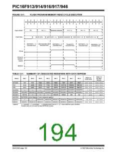
To read a program memory location, the user must
write two bytes of the address to the EEADRL and
EEADRH registers, set the EEPGD control bit, and
then set control bit RD of the EECON1 register. Once
the read control bit is set, the program memory Flash
controller will use the second instruction cycle to read
the data. This causes the second instruction immedi-
ately following the “BSF EECON1,RD” instruction to be
ignored. The data is available in the very next cycle, in
the EEDATL and EEDATH registers; therefore, it can
be read as two bytes in the following instructions.
EEDATL and EEDATH registers will hold this value until
another read or until it is written to by the user (during
a write operation).
Note 1: The two instructions following a program
memory read are required to be NOP’s.
This prevents the user from executing a
two-cycle instruction on the next
instruction after the RD bit is set.
2: If the WR bit is set when EEPGD = 1, the
WR bit will be immediately reset to ‘0’ and
no operation will take place.
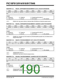
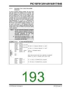
EXAMPLE 13-3:
FLASH PROGRAM READ
BANKSEL EEADRL
;
MOVLW
MOVWF
MOVLW
MOVWF
MS_PROG_EE_ADDR;
EEADRH
;MS Byte of Program Address to read
LS_PROG_EE_ADDR;
EEADRL
;LS Byte of Program Address to read
BANKSEL EECON1
;
BSF
BSF
EECON1, EEPGD ;Point to PROGRAM memory
EECON1, RD
;EE Read
;
;
NOP
NOP
;Any instructions here are ignored as program
;memory is read in second cycle after BSF
BANKSEL EEDATL
;
MOVF
EEDATL, W
;W = LS Byte of EEPROM Data program
MOVWF
MOVF
MOVWF
DATAL
EEDATH, W
DATAH
;
;W = MS Byte of EEPROM Data program
;
© 2007 Microchip Technology Inc.
DS41250F-page 191

 MICROCHIP [ MICROCHIP ]