PIC16F716
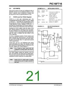
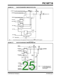
FIGURE 3-6:
BLOCK DIAGRAM OF RB3/CCP1/P1A PIN
VDD
weak
RBPU(1)
[PWMA(P1A) / CCP1 Compare] Output Enable
VDD
P
pull-up
[PWMA(P1A) / CCP1 Compare] Output
PWMA(P1A) Auto-shutdown tri-state
1
0
RB3/CCP1/P1A
VSS
Data Latch
DATA BUS
D
Q
WR PORTB
Q
CK
TRIS Latch
D
Q
WR TRISB
RD TRIS
CK
Q
TTL Buffer
Q
D
EN
RD PORTB
Schmitt Trigger Buffer
CCP – Capture input
Note 1: To enable weak pull-ups, set the appropriate TRIS bit(s) and clear the RBPU bit (OPTION register).
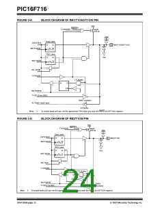
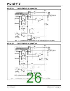
FIGURE 3-7:
BLOCK DIAGRAM OF RB4/ECCPAS0 PIN
VDD
RBPU(1)
VDD
weak
P
pull-up
Data Latch
DATA BUS
RB4/ECCPAS0
D
Q
WR PORTB
CK
TRIS Latch
D
Q
VSS
WR TRISB
TTL
Buffer
CK
ST
Buffer
RD TRIS
Latch
Q
Q
D
EN
Q1
RD PORT
Set RBIF
D
From other
RB<7:4> pins
Note 1: To enable weak pull-ups, set
the appropriate TRIS bit(s)
and clear the RBPU bit of the
OPTION register.
RD PORT
Q3
EN
ECCPAS0: ECCP Auto-Shutdown input
© 2007 Microchip Technology Inc.
DS41206B-page 23

 MICROCHIP [ MICROCHIP ]