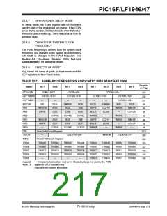
PIC16F/LF1946/47
When TMRx is equal to PRx, the following three events
occur on the next increment cycle:
22.3.2
SETUP FOR PWM OPERATION
The following steps should be taken when configuring
the CCP module for standard PWM operation:
• TMRx is cleared
• The CCPx pin is set. (Exception: If the PWM duty
cycle = 0%, the pin will not be set.)
1. Disable the CCPx pin output driver by setting the
associated TRIS bit.
• The PWM duty cycle is latched from CCPRxL into
CCPRxH.
2. Load the PRx register with the PWM period
value.
3. Configure the CCP module for the PWM mode
by loading the CCPxCON register with the
appropriate values.
Note:
The Timer postscaler (see Section 21.0
“Timer2/4/6 Modules”) is not used in the
determination of the PWM frequency.
4. Load the CCPRxL register and the DCxBx bits
of the CCPxCON register, with the PWM duty
cycle value.
22.3.5
PWM DUTY CYCLE
The PWM duty cycle is specified by writing a 10-bit
value to multiple registers: CCPRxL register and
DCxB<1:0> bits of the CCPxCON register. The
CCPRxL contains the eight MSbs and the DCxB<1:0>
bits of the CCPxCON register contain the two LSbs.
CCPRxL and DCxB<1:0> bits of the CCPxCON
register can be written to at any time. The duty cycle
value is not latched into CCPRxH until after the period
completes (i.e., a match between PRx and TMRx
registers occurs). While using the PWM, the CCPRxH
register is read-only.
5. Configure and start Timer2/4/6:
• Select the Timer2/4/6 resource to be used
for PWM generation by setting the
CxTSEL<1:0> bits in the CCPTMRSx
register.
• Clear the TMRxIF interrupt flag bit of the
PIRx register. See Note below.
• Configure the TxCKPS bits of the TxCON
register with the Timer prescale value.
• Enable the Timer by setting the TMRxON
bit of the TxCON register.
Equation 22-2 is used to calculate the PWM pulse
width.
6. Enable PWM output pin:
• Wait until the Timer overflows and the
TMRxIF bit of the PIRx register is set. See
Note below.
Equation 22-2 is used to calculate the PWM duty cycle
ratio.
• Enable the CCPx pin output driver by clear-
ing the associated TRIS bit.
EQUATION 22-2: PULSE WIDTH
Pulse Width = CCPRxL:CCPxCON<5:4>
TOSC (TMRx Prescale Value)
Note:
In order to send a complete duty cycle and
period on the first PWM output, the above
steps must be included in the setup
sequence. If it is not critical to start with a
complete PWM signal on the first output,
then step 6 may be ignored.
EQUATION 22-3: DUTY CYCLE RATIO
22.3.3
TIMER2/4/6 TIMER RESOURCE
CCPRxL:CCPxCON<5:4>
Duty Cycle Ratio = ----------------------------------------------------------------------
4PRx + 1
The PWM standard mode makes use of one of the 8-bit
Timer2/4/6 timer resources to specify the PWM period.
The CCPRxH register and a 2-bit internal latch are
used to double buffer the PWM duty cycle. This double
buffering is essential for glitchless PWM operation.
Configuring the CxTSEL<1:0> bits in the CCPTMRSx
register selects which Timer2/4/6 timer is used.
22.3.4
PWM PERIOD
The 8-bit timer TMRx register is concatenated with either
the 2-bit internal system clock (FOSC), or 2 bits of the
prescaler, to create the 10-bit time base. The system
clock is used if the Timer2/4/6 prescaler is set to 1:1.
The PWM period is specified by the PRx register of
Timer2/4/6. The PWM period can be calculated using
the formula of Equation 22-1.
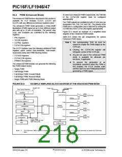
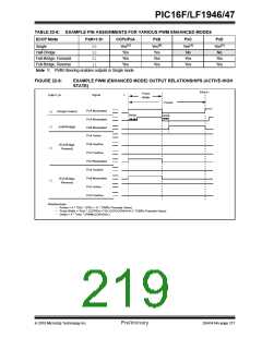
When the 10-bit time base matches the CCPRxH and
2-bit latch, then the CCPx pin is cleared (see
Figure 22-4).
EQUATION 22-1: PWM PERIOD
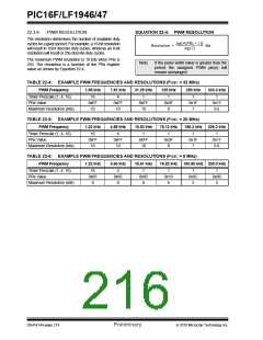
PWM Period = PRx + 1 4 TOSC
(TMRx Prescale Value)
Note 1: TOSC = 1/FOSC
2010 Microchip Technology Inc.
Preliminary
DS41414A-page 213

 MICROCHIP [ MICROCHIP ]