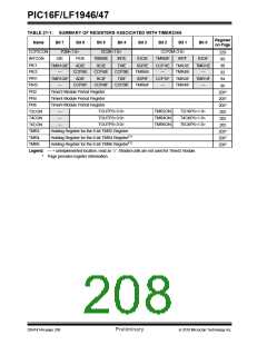
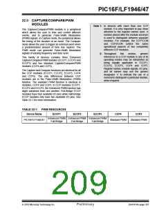
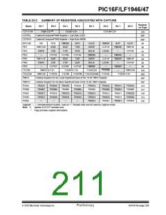
PIC16F/LF1946/47
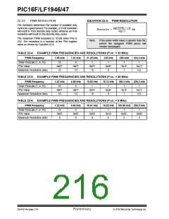
22.2.2
TIMER1 MODE RESOURCE
22.2 Compare Mode
In Compare mode, Timer1 must be running in either
Timer mode or Synchronized Counter mode. The
compare operation may not work in Asynchronous
Counter mode.
The Compare mode function described in this section
is available and identical for CCP modules ECCP1,
ECCP2, ECCP3, CCP4 and CCP5.
Compare mode makes use of the 16-bit Timer1
resource. The 16-bit value of the CCPRxH:CCPRxL
register pair is constantly compared against the 16-bit
value of the TMR1H:TMR1L register pair. When a
match occurs, one of the following events can occur:
See Section 20.0 “Timer1 Module with Gate Control”
for more information on configuring Timer1.
Note:
Clocking Timer1 from the system clock
(FOSC) should not be used in Capture
mode. In order for Capture mode to
recognize the trigger event on the CCPx
pin, TImer1 must be clocked from the
instruction clock (FOSC/4) or from an
external clock source.
• Toggle the CCPx output
• Set the CCPx output
• Clear the CCPx output
• Generate a Special Event Trigger
• Generate a Software Interrupt
22.2.3
SOFTWARE INTERRUPT MODE
The action on the pin is based on the value of the
CCPxM<3:0> control bits of the CCPxCON register. At
the same time, the interrupt flag CCPxIF bit is set.
When Generate Software Interrupt mode is chosen
(CCPxM<3:0> = 1010), the CCPx module does not
assert control of the CCPx pin (see the CCPxCON
register).
All Compare modes can generate an interrupt.
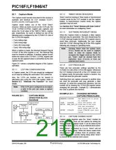
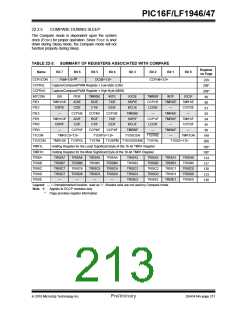
Figure 22-2 shows
Compare operation.
a simplified diagram of the
22.2.4
SPECIAL EVENT TRIGGER
When Special Event Trigger mode is chosen
(CCPxM<3:0> = 1011), the CCPx module does the
following:
FIGURE 22-2:
COMPARE MODE
OPERATION BLOCK
DIAGRAM
• Resets Timer1
CCPxM<3:0>
Mode Select
• Starts an ADC conversion if ADC is enabled
(CCP5 only)
Set CCPxIF Interrupt Flag
The CCPx module does not assert control of the CCPx
pin in this mode.
(PIRx)
4
CCPx
Pin
CCPRxH CCPRxL
Comparator
The Special Event Trigger output of the CCP occurs
immediately upon a match between the TMR1H,
TMR1L register pair and the CCPRxH, CCPRxL
register pair. The TMR1H, TMR1L register pair is not
reset until the next rising edge of the Timer1 clock. The
Special Event Trigger output starts an A/D conversion
(if the A/D module is enabled). This feature is only
available on CCP5. This allows the CCPRxH, CCPRxL
Q
S
R
Output
Logic
Match
TMR1H TMR1L
TRIS
Output Enable
Special Event Trigger
Special Event Trigger will:
register pair to effectively provide
programmable period register for Timer1.
a
16-bit
•
•
CCP<4:1>: Reset Timer1, but not set interrupt flag bit
TMR1IF.
CCP5: Reset Timer1, but not set interrupt flag bit and set bit
GO/DONE (ADCON0<1>).
Note 1: The Special Event Trigger from the CCP
module does not set interrupt flag bit
TMR1IF of the PIR1 register.
22.2.1
CCP PIN CONFIGURATION
2: Removing the match condition by
changing the contents of the CCPRxH
and CCPRxL register pair, between the
clock edge that generates the Special
Event Trigger and the clock edge that
generates the Timer1 Reset, will preclude
the Reset from occurring.
The user must configure the CCPx pin as an output by
clearing the associated TRIS bit.
Also, the CCPx pin function can be moved to
alternative pins using the APFCON register. Refer to
Section 12.1 “Alternate Pin Function” for more
details.
Note:
Clearing the CCPxCON register will force
the CCPx compare output latch to the
default low level. This is not the PORT I/O
data latch.
DS41414A-page 210
Preliminary
2010 Microchip Technology Inc.

 MICROCHIP [ MICROCHIP ]