PIC16F/LF1946/47
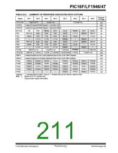
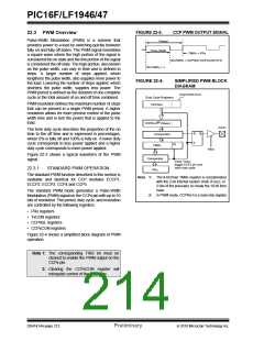
FIGURE 22-3:
CCP PWM OUTPUT SIGNAL
22.3 PWM Overview
Pulse-Width Modulation (PWM) is a scheme that
provides power to a load by switching quickly between
fully on and fully off states. The PWM signal resembles
a square wave where the high portion of the signal is
considered the on state and the low portion of the signal
is considered the off state. The high portion, also known
as the pulse width, can vary in time and is defined in
steps. A larger number of steps applied, which
lengthens the pulse width, also supplies more power to
the load. Lowering the number of steps applied, which
shortens the pulse width, supplies less power. The
PWM period is defined as the duration of one complete
cycle or the total amount of on and off time combined.
Period
Pulse Width
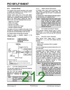
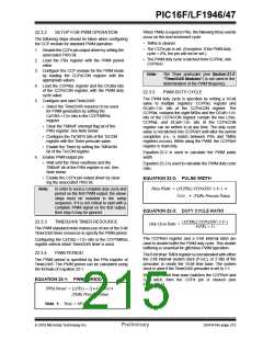
TMRx = PRx
TMRx = CCPRxH:CCPxCON<5:4>
TMRx = 0
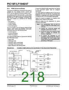
FIGURE 22-4:
SIMPLIFIED PWM BLOCK
DIAGRAM
CCPxCON<5:4>
Duty Cycle Registers
PWM resolution defines the maximum number of steps
that can be present in a single PWM period. A higher
resolution allows for more precise control of the pulse
width time and in turn the power that is applied to the
load.
CCPRxL
CCPRxH(2) (Slave)
Comparator
CCPx
The term duty cycle describes the proportion of the on
time to the off time and is expressed in percentages,
where 0% is fully off and 100% is fully on. A lower duty
cycle corresponds to less power applied and a higher
duty cycle corresponds to more power applied.
R
S
Q
(1)
TMRx
TRIS
Figure 22-3 shows a typical waveform of the PWM
signal.
Comparator
PRx
Clear Timer,
toggle CCPx pin and
latch duty cycle
22.3.1
STANDARD PWM OPERATION
The standard PWM function described in this section is
available and identical for CCP modules ECCP1,
ECCP2, ECCP3, CCP4 and CCP5.
Note 1: The 8-bit timer TMRx register is concatenated
with the 2-bit internal system clock (FOSC), or
2 bits of the prescaler, to create the 10-bit time
base.
The standard PWM mode generates a Pulse-Width
Modulation (PWM) signal on the CCPx pin with up to 10
bits of resolution. The period, duty cycle, and resolution
are controlled by the following registers:
2: In PWM mode, CCPRxH is a read-only register.
• PRx registers
• TxCON registers
• CCPRxL registers
• CCPxCON registers
Figure 22-4 shows a simplified block diagram of PWM
operation.
Note 1: The corresponding TRIS bit must be
cleared to enable the PWM output on the
CCPx pin.
2: Clearing the CCPxCON register will
relinquish control of the CCPx pin.
DS41414A-page 212
Preliminary
2010 Microchip Technology Inc.

 MICROCHIP [ MICROCHIP ]