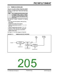
PIC16F/LF1946/47
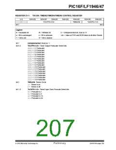
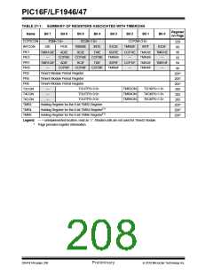
TABLE 21-1: SUMMARY OF REGISTERS ASSOCIATED WITH TIMER2/4/6
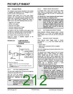
Register
on Page
Name
Bit 7
Bit 6
Bit 5
Bit 4
Bit 3
Bit 2
Bit 1
Bit 0
CCP2CON
INTCON
PIE1
P2M<1:0>
DC2B<1:0>
CCP2M<3:0>
229
89
GIE
PEIE
TMR0IE
INTE
IOCIE
TMR0IF
INTF
IOCIF
TMR1GIE
—
ADIE
RCIE
TXIE
SSPIE
CCP1IE TMR2IE
TMR1IE
—
90
PIE3
CCP5IE
CCP4IE
CCP3IE
TMR6IE
—
TMR4IE
92
PIR1
TMR1GIF
—
ADIF
RCIF
TXIF
SSPIF
CCP1IF
—
TMR2IF
TMR4IF
TMR1IF
—
94
PIR3
CCP5IF
CCP4IF
CCP3IF
TMR6IF
96
PR2
Timer2 Module Period Register
Timer4 Module Period Register
Timer6 Module Period Register
203*
203*
203*
205
205
205
203*
203*
203*
PR4
PR6
T2CON
T4CON
T6CON
TMR2
TMR4
TMR6
—
—
—
TOUTPS<3:0>
TOUTPS<3:0>
TOUTPS<3:0>
TMR2ON
TMR4ON
TMR6ON
T2CKPS<1:0>
T4CKPS<1:0>
T6CKPS<1:0>
Holding Register for the 8-bit TMR2 Register
Holding Register for the 8-bit TMR4 Register(1)
Holding Register for the 8-bit TMR6 Register(1)
Legend: — = unimplemented location, read as ‘0’. Shaded cells are not used for Timer2 module.
Page provides register information.
*
DS41414A-page 206
Preliminary
2010 Microchip Technology Inc.

 MICROCHIP [ MICROCHIP ]