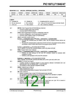
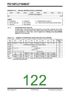
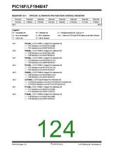
PIC16F/LF1946/47
12.2.2
PORTA FUNCTIONS AND OUTPUT
PRIORITIES
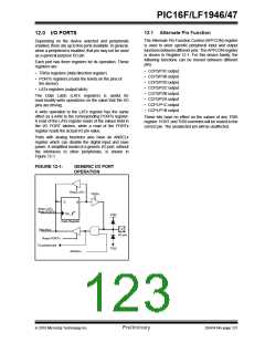
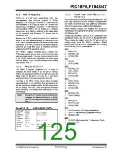
12.2 PORTA Registers
PORTA is a 8-bit wide, bidirectional port. The
corresponding data direction register is TRISA
(Register 12-3). Setting a TRISA bit (= 1) will make the
corresponding PORTA pin an input (i.e., disable the
output driver). Clearing a TRISA bit (= 0) will make the
corresponding PORTA pin an output (i.e., enables
output driver and puts the contents of the output latch
on the selected pin). Example 12-1 shows how to
initialize PORTA.
Each PORTA pin is multiplexed with other functions. The
pins, their combined functions and their output priorities
are briefly described here. For additional information,
refer to the appropriate section in this data sheet.
When multiple outputs are enabled, the actual pin
control goes to the peripheral with the lowest number in
the following lists.
Analog input functions, such as ADC, comparator and
CapSense inputs, are not shown in the priority lists.
These inputs are active when the I/O pin is set for
Analog mode using the ANSELx registers. Digital
output functions may control the pin when it is in Analog
mode with the priority shown below.
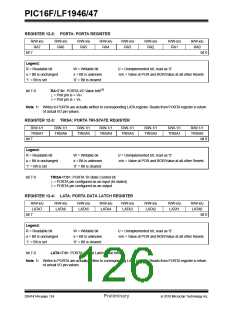
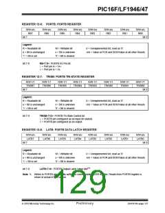
Reading the PORTA register (Register 12-2) reads the
status of the pins, whereas writing to it will write to the
PORT latch. All write operations are read-modify-write
operations. Therefore, a write to a port implies that the
port pins are read, this value is modified and then
written to the PORT data latch (LATA).
RA0
1. AN0 (ADC)
2. SEG33 (LCD)
3. CPS0 (CSM)
The TRISA register (Register 12-3) controls the
PORTA pin output drivers, even when they are being
used as analog inputs. The user should ensure the bits
in the TRISA register are maintained set when using
them as analog inputs. I/O pins configured as analog
input always read ‘0’.
RA1
1. SEG18
2. CPS1 (CSM)
RA2
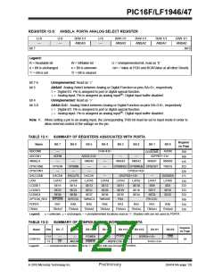
12.2.1
ANSELA REGISTER
1. SEG34 (LCD)
2. VREF- (DAC)
3. AN2 (ADC)
4. CPS2 (CSM)
The ANSELA register (Register 12-5) is used to
configure the Input mode of an I/O pin to analog.
Setting the appropriate ANSELA bit high will cause all
digital reads on the pin to be read as ‘0’ and allow
analog functions on the pin to operate correctly.
RA3
1. VREF+ (DAC)
2. SEG35 (LCD)
3. AN3 (ADC)
4. CPS3 (CSM)
The state of the ANSELA bits has no affect on digital
output functions. A pin with TRIS clear and ANSEL set
will still operate as a digital output, but the Input mode
will be analog. This can cause unexpected behavior
when executing read-modify-write instructions on the
affected port.
RA4
1. SEG14 (LCD)
2. T0CKI (TMR0)
Note:
The ANSELA register must be initialized to
configure an analog channel as a digital
input. Pins configured as analog inputs will
read ‘0’.
RA5
1. AN4 (ADC)
2. SEG15 (LCD)
3. CPS4 (CSM)
RA6
EXAMPLE 12-1:
INITIALIZING PORTA
1. OSC2 (enabled by Configuration Word)
2. CLKOUT (enabled by Configuration Word)
3. SEG36 (LCD)
BANKSEL PORTA
;
CLRF
BANKSEL LATA
CLRF LATA
BANKSEL ANSELA
CLRF ANSELA
BANKSEL TRISA
PORTA
;Init PORTA
;Data Latch
;
;
;digital I/O
;
RA7
1. OSC1/CLKIN (enabled by Configuration Word)
2. SEG37 (LCD)
MOVLW
MOVWF
B'11110000' ;Set RA<7:4> as inputs
TRISA
;and set RA<3:0> as
;outputs
2010 Microchip Technology Inc.
Preliminary
DS41414A-page 123

 MICROCHIP [ MICROCHIP ]