PIC16F/LF1946/47
12.3.3
PORTB FUNCTIONS AND OUTPUT
PRIORITIES
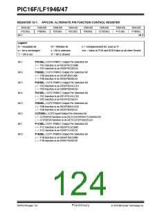
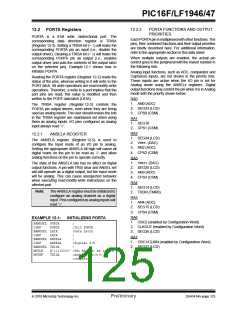
12.3 PORTB Registers
PORTB is an 8-bit wide, bidirectional port. The
corresponding data direction register is TRISB
(Register 12-7). Setting a TRISB bit (= 1) will make the
corresponding PORTB pin an input (i.e., put the
corresponding output driver in a High-Impedance mode).
Clearing a TRISB bit (= 0) will make the corresponding
PORTB pin an output (i.e., enable the output driver and
put the contents of the output latch on the selected pin).
Example 12-2 shows how to initialize PORTB.
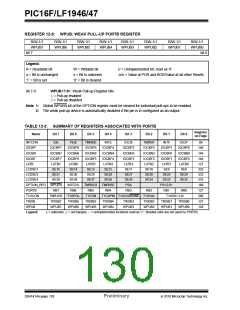
Each PORTB pin is multiplexed with other functions. The
pins, their combined functions and their output priorities
are briefly described here. For additional information,
refer to the appropriate section in this data sheet.
When multiple outputs are enabled, the actual pin
control goes to the peripheral with the lowest number in
the following lists.
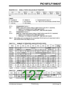
Analog input and some digital input functions are not
included in the list below. These input functions can
remain active when the pin is configured as an output.
Certain digital input functions, such as the EUSART RX
signal, override other port functions and are included in
the priority list.
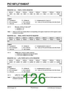
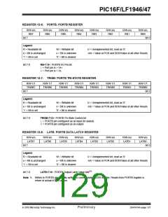
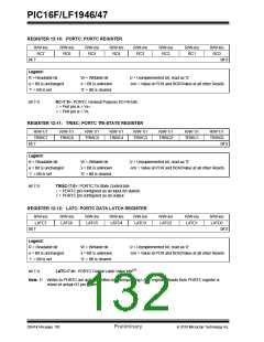
Reading the PORTB register (Register 12-6) reads the
status of the pins, whereas writing to it will write to the
PORT latch. All write operations are read-modify-write
operations. Therefore, a write to a port implies that the
port pins are read, this value is modified and then written
to the PORT data latch (LATB).
RB0
The TRISB register (Register 12-7) controls the PORTB
pin output drivers, even when they are being used as
analog inputs. The user should ensure the bits in the
TRISB register are maintained set when using them as
analog inputs. I/O pins configured as analog input always
read ‘0’.
1. SEG30 (LCD)
2. FLT0 (CCP)
3. SRI (SR Latch)
4. INT
RB1
12.3.1
WEAK PULL-UPS
1. SEG8 (LCD)
RB2
Each of the PORTB pins has an individually configurable
internal weak pull-up. Control bits WPUB<7:0> enable or
disable each pull-up (see Register 12-9). Each weak
pull-up is automatically turned off when the port pin is
configured as an output. All pull-ups are disabled on a
Power-on Reset by the WPUEN bit of the OPTION
register.
1. SEG9 (LCD)
RB3
1. SEG10 (LCD)
RB4
1. SEG11 (LCD)
RB5
12.3.2
INTERRUPT-ON-CHANGE
All of the PORTB pins are individually configurable as
an interrupt-on-change pin. Control bits IOCB<7:0>
enable or disable the interrupt function for each pin.
The interrupt-on-change feature is disabled on a
1. SEG29 (LCD)
2. T1G (TMR1)
RB6
Power-on
Reset.
Reference
Section 13.0
1. ICSPCLK (Programming)
2. ICDCLK (enabled by Configuration Word)
3. SEG38 (LCD)
“Interrupt-On-Change” for more information.
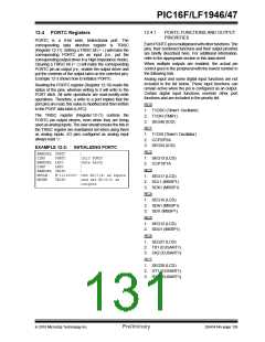
EXAMPLE 12-2:
INITIALIZING PORTB
BANKSEL PORTDB;
RB7
CLRF
BANKSEL LATDB
CLRF LATB
BANKSEL TRISD
PORTB
;Init PORTD
;Data Latch
;
;
1. ICSPDAT (Programming)
2. ICDDAT (enabled by Configuration Word)
3. SEG39 (LCD)
MOVLW
MOVWF
B'11110000' ;Set RD<7:4> as inputs
TRISD
;and set RD<3:0> as
;outputs
DS41414A-page 126
Preliminary
2010 Microchip Technology Inc.

 MICROCHIP [ MICROCHIP ]