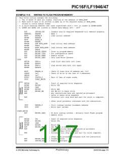
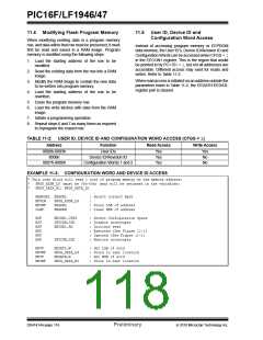
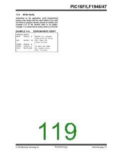
PIC16F/LF1946/47
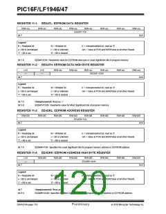
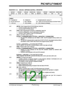
REGISTER 11-5: EECON1: EEPROM CONTROL 1 REGISTER
R/W-0/0
EEPGD
R/W-0/0
CFGS
R/W-0/0
LWLO
R/W/HC-0/0
FREE
R/W-x/q
WRERR
R/W-0/0
WREN
R/S/HC-0/0 R/S/HC-0/0
WR RD
bit 7
bit 0
Legend:
R = Readable bit
W = Writable bit
x = Bit is unknown
‘0’ = Bit is cleared
U = Unimplemented bit, read as ‘0’
S = Bit can only be set
‘1’ = Bit is set
-n/n = Value at POR and BOR/Value at all other Resets
HC = Bit is cleared by hardware
bit 7
bit 6
bit 5
EEPGD: Flash Program/Data EEPROM Memory Select bit
1= Accesses program space Flash memory
0= Accesses data EEPROM memory
CFGS: Flash Program/Data EEPROM or Configuration Select bit
1= Accesses Configuration, User ID and Device ID Registers
0= Accesses Flash Program or data EEPROM Memory
LWLO: Load Write Latches Only bit
If CFGS = 1(Configuration space) OR CFGS = 0and EEPGD = 1 (program Flash):
1= The next WR command does not initiate a write; only the program memory latches are
updated.
0= The next WR command writes a value from EEDATH:EEDATL into program memory latches
and initiates a write of all the data stored in the program memory latches.
If CFGS = 0and EEPGD = 0: (Accessing data EEPROM)
LWLO is ignored. The next WR command initiates a write to the data EEPROM.
bit 4
FREE: Program Flash Erase Enable bit
If CFGS = 1(Configuration space) OR CFGS = 0and EEPGD = 1 (program Flash):
1= Performs an erase operation on the next WR command (cleared by hardware after
completion of erase).
0= Performs a write operation on the next WR command.
If EEPGD = 0 and CFGS = 0: (Accessing data EEPROM)
FREE is ignored. The next WR command will initiate both a erase cycle and a write cycle.
bit 3
WRERR: EEPROM Error Flag bit
1= Condition indicates an improper program or erase sequence attempt or termination (bit is set
automatically on any set attempt (write ‘1’) of the WR bit).
0= The program or erase operation completed normally.
bit 2
bit 1
WREN: Program/Erase Enable bit
1= Allows program/erase cycles
0= Inhibits programming/erasing of program Flash and data EEPROM
WR: Write Control bit
1= Initiates a program Flash or data EEPROM program/erase operation.
The operation is self-timed and the bit is cleared by hardware once operation is complete.
The WR bit can only be set (not cleared) in software.
0= Program/erase operation to the Flash or data EEPROM is complete and inactive.
bit 0
RD: Read Control bit
1= Initiates an program Flash or data EEPROM read. Read takes one cycle. RD is cleared in
hardware. The RD bit can only be set (not cleared) in software.
0= Does not initiate a program Flash or data EEPROM data read.
2010 Microchip Technology Inc.
Preliminary
DS41414A-page 119

 MICROCHIP [ MICROCHIP ]