PIC16F/LF1946/47
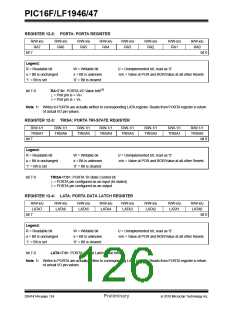
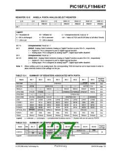
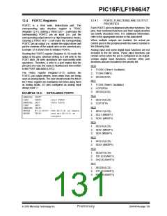
REGISTER 12-5: ANSELA: PORTA ANALOG SELECT REGISTER
U-0
—
U-0
—
R/W-1/1
ANSA5
U-0
—
R/W-1/1
ANSA3
R/W-1/1
ANSA2
R/W-1/1
ANSA1
R/W-1/1
ANSA0
bit 7
bit 0
Legend:
R = Readable bit
W = Writable bit
x = Bit is unknown
‘0’ = Bit is cleared
U = Unimplemented bit, read as ‘0’
-n/n = Value at POR and BOR/Value at all other Resets
u = Bit is unchanged
‘1’ = Bit is set
bit 7-6
bit 5
Unimplemented: Read as ‘0’
ANSA5: Analog Select between Analog or Digital Function on pins RA<5>, respectively
0= Digital I/O. Pin is assigned to port or digital special function.
1= Analog input. Pin is assigned as analog input(1). Digital input buffer disabled.
bit 4
Unimplemented: Read as ‘0’
bit 3-0
ANSA<3:0>: Analog Select between Analog or Digital Function on pins RA<3:0>, respectively
0= Digital I/O. Pin is assigned to port or digital special function.
1= Analog input. Pin is assigned as analog input(1). Digital input buffer disabled.
Note 1: When setting a pin to an analog input, the corresponding TRIS bit must be set to Input mode in order to
allow external control of the voltage on the pin.
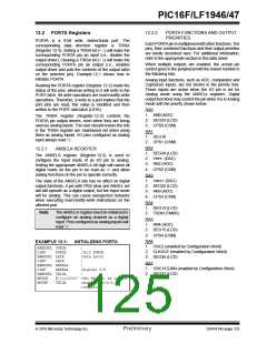
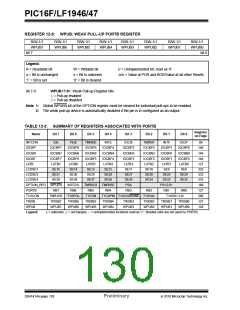
TABLE 12-1: SUMMARY OF REGISTERS ASSOCIATED WITH PORTA
Register
on Page
Name
Bit 7
Bit 6
Bit 5
Bit 4
Bit 3
Bit 2
Bit 1
Bit 0
ADCON0
ADCON1
ANSELA
—
ADFM
—
CHS<4:0>
ADON
GO/DONE
159
160
ADCS<2:0>
ANSA5
—
—
ADPREF<1:0>
—
—
—
ANSA3
ANSA2
ANSA1
ANSA0
T0XCS
125
323
324
171
124
333
333
333
189
124
124
CPSCON0
CPSCON1
DACCON0
LATA
CPSON
—
CPSRM
—
—
—
CPSRNG1 CPSRNG0 CPSOUT
CPSCH<4:0>
DACEN
LATA7
SE15
DACLPS
LATA6
SE14
DACOE
LATA5
SE13
SE21
SE37
TMR0CS
RA5
---
DACPSS<1:0>
---
DACNSS
LATA0
SE8
LATA4
SE12
LATA3
LATA2
SE10
SE18
SE34
LATA1
SE9
LCDSE1
LCDSE2
LCDSE4
OPTION_REG
PORTA
SE11
SE19
SE35
PSA
SE23
SE22
SE20
SE17
SE33
PS<2:0>
RA1
SE16
SE39
SE38
SE36
SE32
WPUEN
RA7
INTEDG
RA6
TMR0SE
RA4
RA3
RA2
RA0
TRISA
TRISA7
TRISA6
TRISA5
TRISA4
TRISA3
TRISA2
TRISA1
TRISA0
Legend:
x= unknown, u= unchanged, – = unimplemented locations read as ‘0’. Shaded cells are not used by PORTA.
TABLE 12-2: SUMMARY OF CONFIGURATION WORD WITH PORTA
Register
on Page
Name
Bits
Bit -/7
Bit -/6
Bit 13/5
Bit 12/4
Bit 11/3
Bit 10/2
Bit 9/1
Bit 8/0
13:8
7:0
—
—
FCMEN
PWRTE
IESO
CLKOUTEN
BOREN<1:0>
FOSC<2:0>
CPD
CONFIG1
54
CP
MCLRE
WDTE<1:0>
Legend:
— = unimplemented location, read as ‘0’. Shaded cells are not used by PORTA.
2010 Microchip Technology Inc.
Preliminary
DS41414A-page 125

 MICROCHIP [ MICROCHIP ]