PIC16F/LF1946/47
12.1 Alternate Pin Function
12.0 I/O PORTS
The Alternate Pin Function Control (APFCON) register
is used to steer specific peripheral input and output
functions between different pins. The APFCON register
is shown in Register 12-1. For this device family, the
following functions can be moved between different
pins.
Depending on the device selected and peripherals
enabled, there are up to five ports available. In general,
when a peripheral is enabled, that pin may not be used
as a general purpose I/O pin.
Each port has three registers for its operation. These
registers are:
• CCP3/P3C output
• CCP3/P3B output
• CCP2/P2D output
• CCP2/P2C output
• CCP2/P2B output
• CCP2/P2A output
• CCP1/P1C output
• CCP1/P1B output
• TRISx registers (data direction register)
• PORTx registers (reads the levels on the pins of
the device)
• LATx registers (output latch)
The Data Latch (LATx registers) is useful for
read-modify-write operations on the value that the I/O
pins are driving.
A write operation to the LATx register has the same
affect as a write to the corresponding PORTx register.
A read of the LATx register reads of the values held in
the I/O PORT latches, while a read of the PORTx
register reads the actual I/O pin value.
These bits have no effect on the values of any TRIS
register. PORT and TRIS overrides will be routed to the
correct pin. The unselected pin will be unaffected.
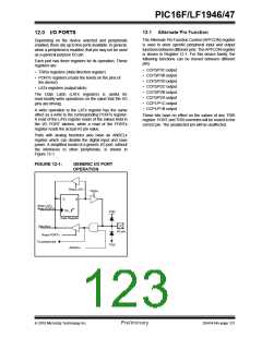
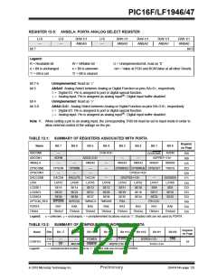
Ports with analog functions also have an ANSELx
register which can disable the digital input and save
power. A simplified model of a generic I/O port, without
the interfaces to other peripherals, is shown in
Figure 12-1.
FIGURE 12-1:
GENERIC I/O PORT
OPERATION
Read LATx
TRISx
D
Q
Write LATx
Write PORTx
CK
Data Register
VDD
Data Bus
Read PORTx
To peripherals
I/O pin
VSS
ANSELx
2010 Microchip Technology Inc.
Preliminary
DS41414A-page 121

 MICROCHIP [ MICROCHIP ]