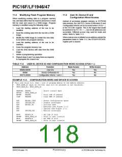
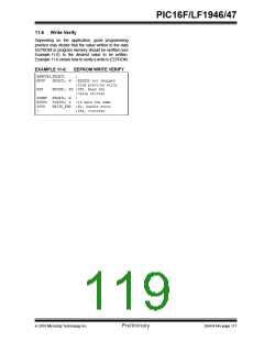
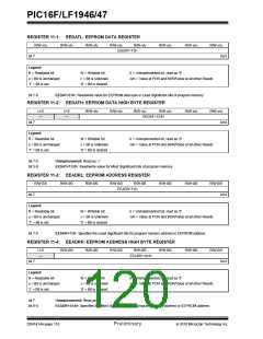
PIC16F/LF1946/47
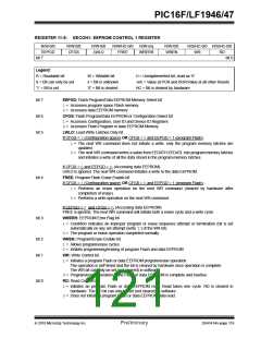
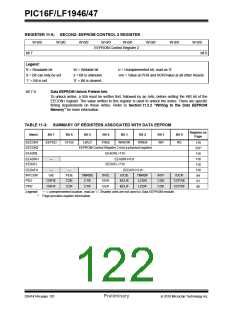
REGISTER 11-6: EECON2: EEPROM CONTROL 2 REGISTER
W-0/0
W-0/0
W-0/0
W-0/0
W-0/0
W-0/0
W-0/0
W-0/0
bit 0
EEPROM Control Register 2
bit 7
Legend:
R = Readable bit
W = Writable bit
x = Bit is unknown
‘0’ = Bit is cleared
U = Unimplemented bit, read as ‘0’
-n/n = Value at POR and BOR/Value at all other Resets
S = Bit can only be set
‘1’ = Bit is set
bit 7-0
Data EEPROM Unlock Pattern bits
To unlock writes, a 55h must be written first, followed by an AAh, before setting the WR bit of the
EECON1 register. The value written to this register is used to unlock the writes. There are specific
timing requirements on these writes. Refer to Section 11.2.2 “Writing to the Data EEPROM
Memory” for more information.
TABLE 11-3: SUMMARY OF REGISTERS ASSOCIATED WITH DATA EEPROM
Register on
Page
Name
Bit 7
Bit 6
Bit 5
Bit 4
Bit 3
Bit 2
Bit 1
Bit 0
EECON1
EECON2
EEADRL
EEPGD
CFGS
LWLO
FREE
WRERR
WREN
WR
RD
119
107*
118
118
118
118
89
EEPROM Control Register 2 (not a physical register)
EEADRL<7:0>
EEADRH
EEDATL
—
EEADRH<6:0
EEDATL<7:0>
EEDATH
INTCON
PIE2
—
—
EEDATH<5:0>
GIE
PEIE
C2IE
C2IF
TMR0IE
C1IE
INTE
EEIE
EEIF
IOCIE
BCLIE
BCLIF
TMR0IF
LCDIE
LCDIF
INTF
C3IE
C3IF
IOCIF
CCP2IE
CCP2IF
OSFIE
OSFIF
91
PIR2
C1IF
95
Legend:
— = unimplemented location, read as ‘0’. Shaded cells are not used by Data EEPROM module.
*
Page provides register information.
DS41414A-page 120
Preliminary
2010 Microchip Technology Inc.

 MICROCHIP [ MICROCHIP ]