PIC16F/LF1946/47
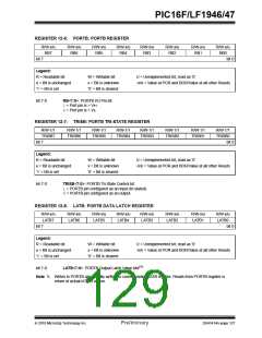
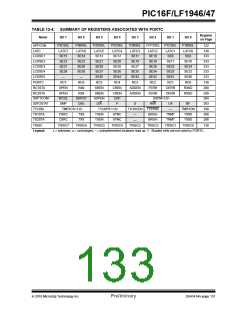
REGISTER 12-6: PORTB: PORTB REGISTER
R/W-x/u
RB7
R/W-x/u
RB6
R/W-x/u
RB5
R/W-x/u
RB4
R/W-x/u
RB3
R/W-x/u
RB2
R/W-x/u
RB1
R/W-x/u
RB0
bit 7
bit 0
Legend:
R = Readable bit
W = Writable bit
U = Unimplemented bit, read as ‘0’
-n/n = Value at POR and BOR/Value at all other Resets
u = Bit is unchanged
‘1’ = Bit is set
x = Bit is unknown
‘0’ = Bit is cleared
bit 7-0
RB<7:0>: PORTB I/O Pin bit
1= Port pin is > VIH
0= Port pin is < VIL
REGISTER 12-7: TRISB: PORTB TRI-STATE REGISTER
R/W-1/1
TRISB7
R/W-1/1
TRISB6
R/W-1/1
TRISB5
R/W-1/1
TRISB4
R/W-1/1
TRISB3
R/W-1/1
TRISB2
R/W-1/1
TRISB1
R/W-1/1
TRISB0
bit 7
bit 0
Legend:
R = Readable bit
W = Writable bit
U = Unimplemented bit, read as ‘0’
-n/n = Value at POR and BOR/Value at all other Resets
u = Bit is unchanged
‘1’ = Bit is set
x = Bit is unknown
‘0’ = Bit is cleared
bit 7-0
TRISB<7:0>: PORTB Tri-State Control bit
1= PORTB pin configured as an input (tri-stated)
0= PORTB pin configured as an output
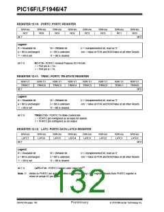
REGISTER 12-8: LATB: PORTB DATA LATCH REGISTER
R/W-x/u
LATB7
R/W-x/u
LATB6
R/W-x/u
LATB5
R/W-x/u
LATB4
R/W-x/u
LATB3
R/W-x/u
LATB2
R/W-x/u
LATB1
R/W-x/u
LATB0
bit 7
bit 0
Legend:
R = Readable bit
W = Writable bit
U = Unimplemented bit, read as ‘0’
-n/n = Value at POR and BOR/Value at all other Resets
u = Bit is unchanged
‘1’ = Bit is set
x = Bit is unknown
‘0’ = Bit is cleared
bit 7-0
LATB<7:0>: PORTB Output Latch Value bits(1)
Note 1: Writes to PORTB are actually written to corresponding LATB register. Reads from PORTB register is
return of actual I/O pin values.
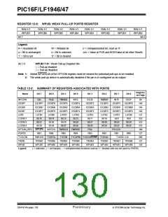
2010 Microchip Technology Inc.
Preliminary
DS41414A-page 127

 MICROCHIP [ MICROCHIP ]