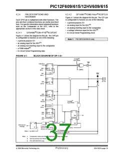
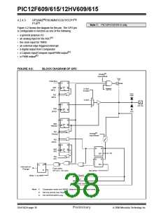
PIC12F609/615/12HV609/615
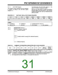
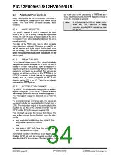
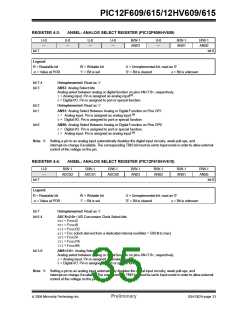
REGISTER 4-3:
ANSEL: ANALOG SELECT REGISTER (PIC12F609/HV609)
U-0
—
U-0
—
U-0
—
U-0
—
R/W-1
ANS3
U-0
—
R/W-1
ANS1
R/W-1
ANS0
bit 7
bit 0
Legend:
R = Readable bit
-n = Value at POR
W = Writable bit
‘1’ = Bit is set
U = Unimplemented bit, read as ‘0’
‘0’ = Bit is cleared x = Bit is unknown
bit 7-4
bit 3
Unimplemented: Read as ‘0’
ANS3: Analog Select bits
Analog select between analog or digital function on pins AN<7:0>, respectively.
(1)
1= Analog input. Pin is assigned as analog input
.
0= Digital I/O. Pin is assigned to port or special function.
bit 2
bit 1
Unimplemented: Read as ‘0’
ANS1: Analog Select Between Analog or Digital Function on Pins GP1
(1)
1= Analog input. Pin is assigned as analog input.
0= Digital I/O. Pin is assigned to port or special function.
bit 0
ANS0: Analog Select Between Analog or Digital Function on Pins GP0
0= Digital I/O. Pin is assigned to port or special function.
1= Analog input. Pin is assigned as analog input.
(1)
Note 1: Setting a pin to an analog input automatically disables the digital input circuitry, weak pull-ups, and
interrupt-on-change if available. The corresponding TRIS bit must be set to Input mode in order to allow external
control of the voltage on the pin.
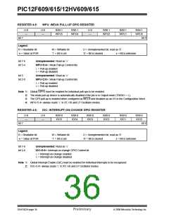
REGISTER 4-4:
ANSEL: ANALOG SELECT REGISTER (PIC12F615/HV615)
U-0
—
R/W-1
R/W-1
R/W-1
R/W-1
ANS3
R/W-1
ANS2
R/W-1
ANS1
R/W-1
ANS0
ADCS2
ADCS1
ADCS0
bit 7
bit 0
Legend:
R = Readable bit
-n = Value at POR
W = Writable bit
‘1’ = Bit is set
U = Unimplemented bit, read as ‘0’
‘0’ = Bit is cleared x = Bit is unknown
bit 7
Unimplemented: Read as ‘0’
bit 6-4
ADCS<2:0>: A/D Conversion Clock Select bits
000= FOSC/2
001= FOSC/8
010= FOSC/32
x11= FRC (clock derived from a dedicated internal oscillator = 500 kHz max)
100= FOSC/4
101= FOSC/16
110= FOSC/64
bit 3-0
ANS<3:0>: Analog Select bits
Analog select between analog or digital function on pins AN<7:0>, respectively.
(1)
1= Analog input. Pin is assigned as analog input
.
0= Digital I/O. Pin is assigned to port or special function.
Note 1: Setting a pin to an analog input automatically disables the digital input circuitry, weak pull-ups, and
interrupt-on-change if available. The corresponding TRIS bit must be set to Input mode in order to allow external
control of the voltage on the pin.
© 2006 Microchip Technology Inc.
Preliminary
DS41302A-page 33

 MICROCHIP [ MICROCHIP ]