PIC12F609/615/12HV609/615
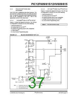
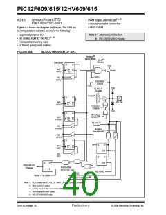
4.2.4.4
GP3/T1G(1, 2)/MCLR/VPP
Figure 4-3 shows the diagram for this pin. The GP3 pin
is configurable to function as one of the following:
• a general purpose input
(1, 2)
• a Timer1 gate (count enable), alternate pin
• as Master Clear Reset with weak pull-up
Note 1: Alternate pin function.
2: PIC12F615/HV615 only.
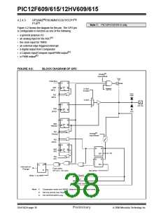
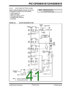
FIGURE 4-3:
BLOCK DIAGRAM OF GP3
VDD
MCLRE
Weak
Data Bus
MCLRE
Reset
Input
Pin
RD
TRISIO
VSS
MCLRE
VSS
RD
GPIO
D
Q
Q
Q
Q
D
CK
WR
IOC
Q1
EN
RD
IOC
D
(1)
Q
S
EN
Interrupt-on-
Change
From other
GP<5:4, 2:0> pins
R
RD GPIO
Write ‘0’ to GBIF
Note 1: Set has priority over Reset
© 2006 Microchip Technology Inc.
Preliminary
DS41302A-page 37

 MICROCHIP [ MICROCHIP ]