PIC12F609/615/12HV609/615
last read value is not affected by a MCLR nor BOR
Reset. After these resets, the GPIF flag will continue to
be set if a mismatch is present.
4.2
Additional Pin Functions
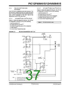
Every GPIO pin on the PIC12F609/615/12HV609/615
has an interrupt-on-change option and a weak pull-up
option. The next three sections describe these
functions.
Note:
If a change on the I/O pin should occur
when any GPIO operation is being
executed, then the GPIF interrupt flag may
not get set.
4.2.1
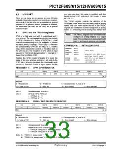
ANSEL REGISTER
The ANSEL register is used to configure the Input
mode of an I/O pin to analog. Setting the appropriate
ANSEL bit high will cause all digital reads on the pin to
be read as ‘0’ and allow analog functions on the pin to
operate correctly.
The state of the ANSEL bits has no affect on digital
output functions. A pin with TRIS clear and ANSEL set
will still operate as a digital output, but the Input mode
will be analog. This can cause unexpected behavior
when executing read-modify-write instructions on the
affected port.
4.2.2
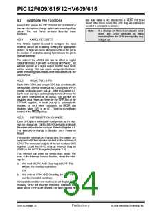
WEAK PULL-UPS
Each of the GPIO pins, except GP3, has an individually
configurable internal weak pull-up. Control bits WPUx
enable or disable each pull-up. Refer to Register 4-5.
Each weak pull-up is automatically turned off when the
port pin is configured as an output. The pull-ups are
disabled on a Power-on Reset by the GPPU bit of the
OPTION register). A weak pull-up is automatically
enabled for GP3 when configured as MCLR and
disabled when GP3 is an I/O. There is no software
control of the MCLR pull-up.
4.2.3
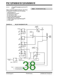
INTERRUPT-ON-CHANGE
Each GPIO pin is individually configurable as an inter-
rupt-on-change pin. Control bits IOCx enable or disable
the interrupt function for each pin. Refer to Register 4-6.
The interrupt-on-change is disabled on a Power-on
Reset.
For enabled interrupt-on-change pins, the values are
compared with the old value latched on the last read of
GPIO. The ‘mismatch’ outputs of the last read are OR’d
together to set the GPIO Change Interrupt Flag bit
(GPIF) in the INTCON register (Register 2-3).
This interrupt can wake the device from Sleep. The
user, in the Interrupt Service Routine, clears the inter-
rupt by:
a) Any read of GPIO AND Clear flag bit GPIF. This
will end the mismatch condition;
OR
b) Any write of GPIO AND Clear flag bit GPIF will
end the mismatch condition;
A mismatch condition will continue to set flag bit GPIF.
Reading GPIO will end the mismatch condition and
allow flag bit GPIF to be cleared. The latch holding the
DS41302A-page 32
Preliminary
© 2006 Microchip Technology Inc.

 MICROCHIP [ MICROCHIP ]