PIC12F609/615/12HV609/615
port pins are read, this value is modified and then
written to the PORT data latch. GP3 reads ‘0’ when
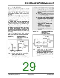
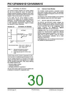
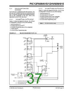
4.0
I/O PORT
There are as many as six general purpose I/O pins
available. Depending on which peripherals are enabled,
some or all of the pins may not be available as general
purpose I/O. In general, when a peripheral is enabled,
the associated pin may not be used as a general
purpose I/O pin.
MCLRE = 1.
The TRISIO register controls the direction of the
GPIO pins, even when they are being used as analog
inputs. The user must ensure the bits in the TRISIO
register are maintained set when using them as analog
inputs. I/O pins configured as analog input always read
‘0’.
4.1
GPIO and the TRISIO Registers
Note:
The ANSEL register must be initialized to
configure an analog channel as a digital
input. Pins configured as analog inputs will
read ‘0’ and cannot generate an interrupt.
GPIO is a 6-bit wide port with 5 bidirectional and 1
input-only pin. The corresponding data direction register
is TRISIO (Register 4-2). Setting a TRISIO bit (= 1) will
make the corresponding GPIO pin an input (i.e., disable
the output driver). Clearing a TRISIO bit (= 0) will make
the corresponding GPIO pin an output (i.e., enables
output driver and puts the contents of the output latch on
the selected pin). The exception is GP3, which is input
only and its TRIS bit will always read as ‘1’. Example 4-1
shows how to initialize GPIO.
EXAMPLE 4-1:
INITIALIZING GPIO
BANKSEL GPIO
;
CLRF
GPIO
;Init GPIO
;
BANKSEL ANSEL
CLRF
ANSEL
;digital I/O, ADC clock
;setting ‘don’t care’
;Set GP<3:2> as inputs
;and set GP<5:4,1:0>
;as outputs
MOVLW
MOVWF
0Ch
TRISIO
Reading the GPIO register (Register 4-1) reads the
status of the pins, whereas writing to it will write to the
PORT latch. All write operations are read-modify-write
operations. Therefore, a write to a port implies that the
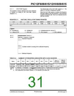
REGISTER 4-1:
GPIO: GPIO REGISTER
U-0
—
U-0
R/W-x
GP5
R/W-0
GP4
R-x
R/W-0
GP2
R/W-0
GP1
R/W-0
GP0
—
GP3
bit 7
bit 0
Legend:
R = Readable bit
-n = Value at POR
W = Writable bit
‘1’ = Bit is set
U = Unimplemented bit, read as ‘0’
‘0’ = Bit is cleared
x = Bit is unknown
bit 7-6
bit 5-0
Unimplemented: Read as ‘0’
GP<5:0>: GPIO I/O Pin bit
1= GPIO pin is > VIH
0= GPIO pin is < VIL
REGISTER 4-2:
TRISIO: GPIO TRI-STATE REGISTER
U-0
—
U-0
—
R/W-1
R/W-1
R-1
R/W-1
R/W-1
R/W-1
TRISIO5
TRISIO4
TRISIO3
TRISIO2
TRISIO1
TRISIO0
bit 0
bit 7
Legend:
R = Readable bit
-n = Value at POR
W = Writable bit
‘1’ = Bit is set
U = Unimplemented bit, read as ‘0’
‘0’ = Bit is cleared x = Bit is unknown
bit 7-6
bit 5-0
Unimplemented: Read as ‘0’
TRISIO<5:0>: GPIO Tri-State Control bit
1= GPIO pin configured as an input (tri-stated)
0= GPIO pin configured as an output
Note 1: TRISIO<3> always reads ‘1’.
2: TRISIO<5:4> always reads ‘1’ in XT, HS and LP Oscillator modes.
© 2006 Microchip Technology Inc.
Preliminary
DS41302A-page 31

 MICROCHIP [ MICROCHIP ]